


Hello everyone,
I had the curious idea to develop my own framework to use the airbooster pack on a Tiva C Launchpad. Basically this board is not pin to pin compliant with the AirBooster pack so step 1 was to design a PCB to route the SSI0 from the TivaC headers to the ABP headers. Actually it only provides pull-up resistors on the SPI lines (MISO, MOSI, SS, SCLK) to make it idle high. => OK it works
Step 2 was to provide a convenient way to send SPI commands so I can measure timings with my oscilloscope. So I started my program based on the usb_dev_serial example to get a Shell via virtual com port. => OK it works, I can decode my command "SPI <length in decimal> <data to send hexa>"
Since I need to setup my SPI driver, I plugged my little adapting PCBA into the TivaC and started using SPI with driverlib ssi module.
In the beginning of "main" function, I call
1. initialization of SPI,
2. initialization of USB
Then goes an infinite loop to manage Shell commands
The problem is that I do not see anything going on the SPI bus, although everything appears to be fine. I went to microcontroller datasheet to know what happens. Here is where my investigation is :
To enable and initialize the SSI, the following steps are necessary:
1. Enable the SSI module using the RCGCSSI register (see page 346).
SYSCTL_RCGCSSI_R0 1 SSI Module 0 Run Mode Clock Gating Control => SSI0 enabled
2. Enable the clock to the appropriate GPIO module via the RCGCGPIO register (see page 340).
To find out which GPIO port to enable, refer to Table 23-5 on page 1351.
SYSCTL_RCGCGPIO_R3 1 GPIO Port D Run Mode Clock Gating Control => USB0
SYSCTL_RCGCGPIO_R0 1 GPIO Port A Run Mode Clock Gating Control => SSI0 : SSI0Clk = A2, SSI0Fss = A3, SSI0Rx = A4, SSI0Tx = A5
3. Set the GPIO AFSEL bits for the appropriate pins (see page 671). To determine which GPIOs to
configure, see Table 23-4 on page 1344.
GPIO_AFSEL 0x0000003C GPIO Alternate Function Select [Memory Mapped]
0b111100 => A2+A3+A4+A5 are linked to alternate function
4. Configure the PMCn fields in the GPIOPCTL register to assign the SSI signals to the appropriate
pins. See page 688 and Table 23-5 on page 1351.
GPIO_PCTL 0x00222211 GPIO Port Control [Memory Mapped]
PMC2 = 0x2 => SSI0
PMC3 = 0x2 => SSI0
PMC4 = 0x2 => SSI0
PMC5 = 0x2 => SSI0
5. Program the GPIODEN register to enable the pin's digital function. In addition, the drive strength,
drain select and pull-up/pull-down functions must be configured. Refer to “General-Purpose
Input/Outputs (GPIOs)” on page 649 for more information.
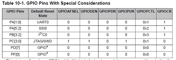
GPIO_DEN 0x0000003C GPIO Digital Enable [Memory Mapped] => The digital functions for the pins A2 to A5 are enabled
=> not clear : should be 0 ??
For each of the frame formats, the SSI is configured using the following steps:
1. Ensure that the SSE bit in the SSICR1 register is clear before making any configuration changes.
SSI_CR1_SSE 0 SSI Synchronous Serial Port Enable
2. Select whether the SSI is a master or slave:
a. For master operations, set the SSICR1 register to 0x0000.0000.
SSI_CR1 0x00000002 SSI Control 1 [Memory Mapped]
SSI_CR1_EOT 0 End of Transmission
SSI_CR1_MS 0 SSI Master/Slave Select
SSI_CR1_SSE 1 SSI Synchronous Serial Port Enable
SSI_CR1_LBM 0 SSI Loopback Mode
=> Fine, I took this right after sending a byte
b. For slave mode (output enabled), set the SSICR1 register to 0x0000.0004.
c. For slave mode (output disabled), set the SSICR1 register to 0x0000.000C.
3. Configure the SSI clock source by writing to the SSICC register.
SSI_CC 0x00000000 SSI Clock Configuration [Memory Mapped]
SSI_CC_CS 0000 - SSI Baud Clock Source
=> 0x0 System clock (based on clock source and divisor factor)
4. Configure the clock prescale divisor by writing the SSICPSR register.
SSI_CPSR 0x00000002 SSI Clock Prescale [Memory Mapped]
SSI_CPSR_CPSDVSR 00000010 SSI Clock Prescale Divisor
=> Divider is 2
5. Write the SSICR0 register with the following configuration:
¦ Serial clock rate (SCR)
¦ Desired clock phase/polarity, if using Freescale SPI mode (SPH and SPO)
¦ The protocol mode: Freescale SPI, TI SSF, MICROWIRE (FRF)
¦ The data size (DSS)
SSI_CR0 0x000018C7 SSI Control 0 [Memory Mapped]
SSI_CR0_SCR 00011000 SSI Serial Clock Rate
=> BR=SysClk/(CPSDVSR * (1 + SCR)) = 50MHz / (2 * (1 + 24)) = 1 MHz
SSI_CR0_SPH 1 SSI Serial Clock Phase
=> Data is captured on the second clock edge transition so Rising edge
SSI_CR0_SPO 1 SSI Serial Clock Polarity
=> Clock is idle HIGH
SSI_CR0_FRF 00 - SSI Frame Format Select
=> Freescale SPI Frame Format
SSI_CR0_DSS 0111 - SSI Data Size Select
=> 8-bit data
6. Optionally, configure the SSI module for µDMA use with the following steps
SSI_DMACTL 0x00000000 SSI DMA Control [Memory Mapped]
=> no DMA
7. Enable the SSI by setting the SSE bit in the SSICR1 register.
SSI_CR1_SSE 1 SSI Synchronous Serial Port Enable
I hope this is enough to help me in my problem. I also provide my code in attachment so you can browse it or test it on an actual board. Hopefully anybody can help me.
My configuration is : CCS V6.1.2 + TivaWare C Series 2.1.2.111
Thank you !
