This thread has been locked.

If you have a related question, please click the "Ask a related question" button in the top right corner. The newly created question will be automatically linked to this question.

Schematic Design For TM4C123GH6PM

Other Parts Discussed in Thread: TM4C123GH6PM

Hi,

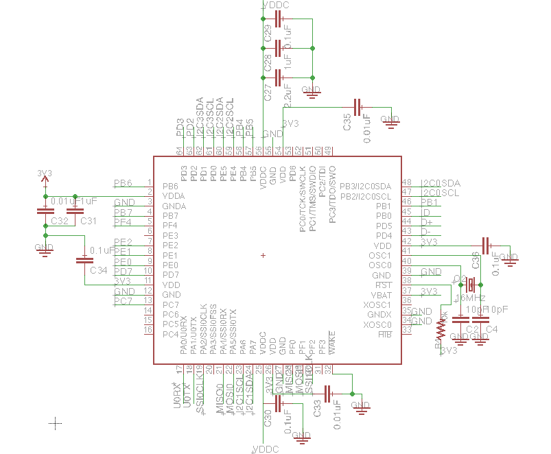
I'm a college student working on a project using TM4C123GH6PM. I built the schematic in EAGLE based on the datasheet for evaluation board but I still have some questions.

In the design guidelines for TM4C123GH6PM, it says:

Decoupling capacitors are typically 0.1 μF in value and should be accompanied by a bulk capacitor near the microcontroller. The combined VDD and VDDA bulk capacitance of the microcontroller is typically between 2 μF and 22 μF.

I don't really know what it means by "bulk capacitance of the microcontroller is typically between 2 μF and 22 μF" cause in the current schematic, the capacitance is smaller than 2 μF. And also, 2 of the capacitors are 0.01μF instead of 0.1 μF.

Does my shcematic look ok as the basic set up? I'm pretty new to microcontrollers so I'm not very sure.


Thank you guys so much!

  • Hello Sylvia,

    A bulk capacitor acts as a supply when there is a high current demand instantaneously before the power supply reacts.

    1. XOSC0 must be connected to GND
    2. JTAG does not show any connectivity. How do you plan to debug the device?

    Regards
    Amit
  • Typically you have a low value capacitance in parallel to the standard decoupling capacitor for improved frequency response. 100nF paralleled with 10nF is fairly common.

    Note that the top diagram you show has a 2u2 capacitor as a local bulk capacitor.

    You end up with hierarchy of capacitors to keep the power supply steady. Small, high frequency near the device, larger lower frequency further away where inductance slows the response all the way to the regulator ant its capacitance.

    This should be discussed in much more detail in your course.

    Robert
  • Hi Robert,
    Do you mean that the 2u2 capacitor connected to VDDC can also count as the VDD and VDDA bulk capacitor for the microcontroller?
    I'm taking microprocessor class in the following school year so I haven't really learned about this.
    Thank you so much for your help!
  • Might it be (fairly) said that, "Forcing such relatively new students - so soon - into MCU pcb layout" is hugely unproductive?   How is it that the schools (so many of them) miss this obvious point?    Would industry - even small tech firms such as mine - ever trust one "so new" in such layout?

    The vast amount of (new) learning forced upon students (or hobbyist) by the complexity of the ARM MCU is quite sufficient - don't we think?   Adding pcb layout to a new user's agenda makes little (perhaps NO) sense!

    Vendor's LPads and/or this/other vendors' Eval Boards are low cost - and built by those experienced & skilled - insuring quality & meeting of design rules/guidelines.   If - and only if - the design requires "special ICs" and/or signal routings - a daughter board (minus fine pitch devices) - proves a far more appropriate use of the new user/student's "pcb" skill & knowledge levels.

  • Hi Amit,

    So do I need to add extra capacitors or the ones connected to VDDC can also count?

    1. I think I connected XOSC0 to GND.
    2. I will make headers for JTAG. Thank you so much for pointing this out!

    Thank you!

    Sylvia
  • Hello Sylvia

    VDDC caps are OK. Make sure that for VDD+VDDA there is one 0.1uF cap per pin and an additional bulk capacitor.

    Regards
    Amit
  • Hi Amit,

    But in the evaluation board schematic, there are two 0.1uF and two 0.01uF for 4 VDD pins. Should I change all of them into 0.1 uF?

    Thank you!

    Sylvia
  • Hello Sylvia

    The LaunchPad is not a product nor is it a reference design. You must refer to the System Design Guidelines document for a PCB design with TM4C123x device.

    www.ti.com/.../spma059.pdf

    Regards
    Amit
  • Perhaps it proves, "Not too much of a reach" to predict that w/in the next few weeks will emerge:

    • A "first time effort" pcb
    • first time effort pcb assembly

    And of course:

    • school dictated "DRM" code - most often (only) sparsely commented

    And this is - in total, "Highly unlikely to work!"   (As hardware (first ever pcb), assembly (fine pitch MCU) and (likely) DRM code all are new, unverified.)     Most successful firms/individuals try to, "Limit the number of variables/unknowns" - in contrast, (here) ALL appear (warmly) welcome!

    Might something be "amiss" with this scenario?    How will the (hapless) novice poster know whether her (issues) are hardware or software?   (or both)   And what about intermittents - what then?   Could we have devised a (more) error-prone undertaking?  (Especially when well tested LPads stand, "At the ready!")

    Is my group (alone) in, "Seeing this coming - wishing to sound an alarm?"   (and should this (premature) effort (really) be encouraged? - by all but one...)

  • Hello cb1

    Agreed and well said. That is where the guidelines come into picture. Has the poster checked the design being "copied" is matching the guidelines. If not then asking the correct questions (which the poster has started taking the path) is the first step.

    Regards
    Amit
  • Amit,

    As you & your fellows answer (so many) MCU issues here - and (by far) most result from very well tested/verified LPads & Eval Boards - how can encouraging a pcb design novice make ANY sense?

    This is NO knock on our poster - but instead firm's/my, "Intruding sense of reality" - which (unfortunately) escapes too many w/in the university structure.   Our poster was "unaware" of the need for JTAG connections & header - was she not?    Is she ready, willing & able to absorb complex, PCB guidelines?    Really?
     
    Seriously - embarking upon a fine-pitch, MCU board design - when hundreds of "Code Examples" are thus "bypassed/neglected" makes NO Sense!   As owner of a small tech firm NEVER/EVER would we direct a pcb design to a novice.   And ALWAYS we'd want them able to effectively solve "real-world" programming and MCU utilization challenges.   I guarantee that there is NOT time to teach & perfect BOTH - not a chance!

    Forcing students into a low-value - highly demanding - design exercise (one they are woefully unprepared to meet) - WHILE sacrificing the very needed programming & problem-solving skills small tech firms NEED - proves destructive - does it not?

    It is only if we "Suspend Disbelief" that this school-directed - far "OFF Mark" home-brew pcb exercise - makes ANY Sense!   We note that the school (apparently) "Could not be bothered" to emphasize the importance of JTAG!    (i.e.   Does this not much ring of, "Lambs to Slaughter?)     (Someone had to say this!)

  • Hello cb1,

    I am not encouraging a pcb design by a novice, but only helping if they need to design one. Clearly design rules are not being taken into account here and would it not be a good way for them to learn that looking at design specifications rather than taking something at the face value is not going to get the intended results.

    Regards
    Amit
  • Hi cb1,

    I understand what you mean by such design is too complicated for a novice like me and I agree, but there are a few misunderstandings.

    1. This project is actually not for school but for my startup. My school doesn't have any PCB design class so I had no idea about microcontroller, not to mention what is JTAG and I learned everything on my own. I know this may seem very unprofessional to you, but I'm trying my best as a 20-year-old kid who'd like to learn. I'm not getting paid for this, so it's more of personal interest and learning experience.
    2. We will pay professionals to do our assembly and the CS people are already working on the coding part with the evaluation board.
    3. I really appreaciate thoes who answered my questions cause that's what I need right now. I do realize my ignorance and that my question is stupid but I still have plenty of time to learn in my education and carrer to be a real engineer.

    However, I still appreaciate that you spent so much time trying to tell me this project is impossible and I believe you mean no harm to someone who wasn't even born when you started to work in this field. At least, I know that it's not really my fault that I don't know about this lol. But anyway, I believe that everyone starts from a novice and you can only become a good engineer after practice and failure. I may have chosen a tough start, but I won't stop cause it's hard.
    If you have any suggestion on how I should start to learn this more systematically (book,video, etc), please feel free to tell me.

    Thank you!

    Sylvia
  • Hi Sylvia,

    Never/ever did I suggest that "you" were unprofessional - nor ignorant, nor that your questions & objectives were "stupid."   I had mistakenly (we now learn) assumed that your school had, "forced such assignment upon you."    And - as noted - that simply overloads any new person - pcb design (good pcb design) is both an "art & science!"   Never/ever for a beginner - especially if they desire a robust, high-performing pcb!

    My goal was to alert you to the fact that learning to exploit the ARM MCU is a demanding & critical task - all on its own.   Simply spend some time here - or at other ARM forums - you'll note so many - crash/burn!    And they use "pro boards!"  

    And - if you are to start with:

    • an untried, untested/verified pcb
    • untried, untested pcb assembly skills
    • equally untried, untested/verified software

    You have created a (deadly) condition which firm/I describe as, "Maximum Randomness!"   How (ever) will you know if your board design, or assembly, or component values or your software cause issues?   Ans: you cannot - that is why I (continue) to press strongly for your development work to be done on a "pro" LPad or Eval board.   Only later - when your software has been test/verified - would I venture to "your own pcb design!"   This greatly removes/reduces you from the "clutches" of "Maximum Randomness."

    Your venture - just like mine - usually must focus on those things you can "uniquely do" and do well.   Becoming expert in ALL AREAS is unlikely - after more than a few decades in this field - I still try to learn - each/every day.  

    Focus is very important - our investors always advise that we "Stick to our expertise" and engage others for the (needed) extra.   Getting your product to work - and to market - surely "trumps" doing everything yourself - and arriving late.  (or last!)   Race is to the swift - profit margins are highest then - huge penalties await those using DRM (worse still - ASM) or doing things "outside of their capability/strength!"

    Wish you well - I am NOT negative - but strongly resist those tactics I KNOW to be inefficient - and often - simply - WRONG!   (and this method/madness enabled me to past co-found, then take tech firm public...)

  • Hello Sylvia

    A lot of inputs taken in the most +ve manner.

    Regards
    Amit