This thread has been locked.

If you have a related question, please click the "Ask a related question" button in the top right corner. The newly created question will be automatically linked to this question.

Input Timing Requirements for Hercules TMS570LS1114

Other Parts Discussed in Thread: TMS570LS1114

Hi TI Experts,

I found in TMS570LS1114 datasheet described as follows

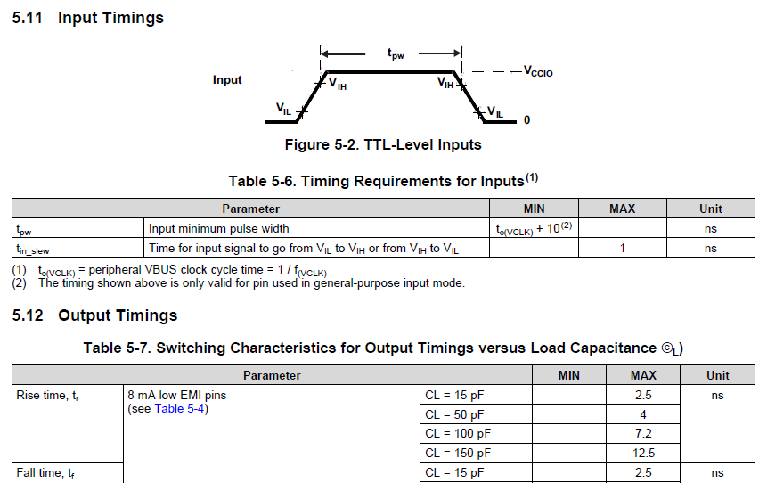
Does this MCU need tin_slew  "Time for input signal to go from VIL to VIH or from VIH to VIL" on every input pin  to be less than 1ns to work properly?

I think this requirement is kind of too strict. On the other hand, we can see the output timings of this MCU, depending on load capacitance, the maximum  Tr or Tf can be as high as 12.5ns, or 2.5ns for Cl = 15pF.

A 2.5ns input slew time will not cause most IC to work abnormally. So why Hercules MCU define a 1ns maximum input slew time?  

  • Nestor,

    Yes although I suspect this means that the other timing requirements for example the SDRAM timings assume a slew rate of <1ns and would be degraded if the slew rate is worse. Thanks for pointing this out I will file a documentation bug.

    -Anthony
  • This is a more specific example of what i think this table is trying to communicate - it's what I am submitting in the defect report for the datasheet:

    'For example, when we specify a parameter such as Parameter 4 of MibSPI slave, 'td(SPCH-SOMI)S' Delay time, SPISOMI valid after SPICLK high...

    This assumes that the transition on the SPI clock is < 1ns and the delay of trf+20ns might be degraded (longer) if the slew rate on the SPI Clock input is slower than 1ns. "