This thread has been locked.

If you have a related question, please click the "Ask a related question" button in the top right corner. The newly created question will be automatically linked to this question.

Reading a HO 10-P Current Sensor with TM4C123 dev board

Other Parts Discussed in Thread: TM4C123GH6PM

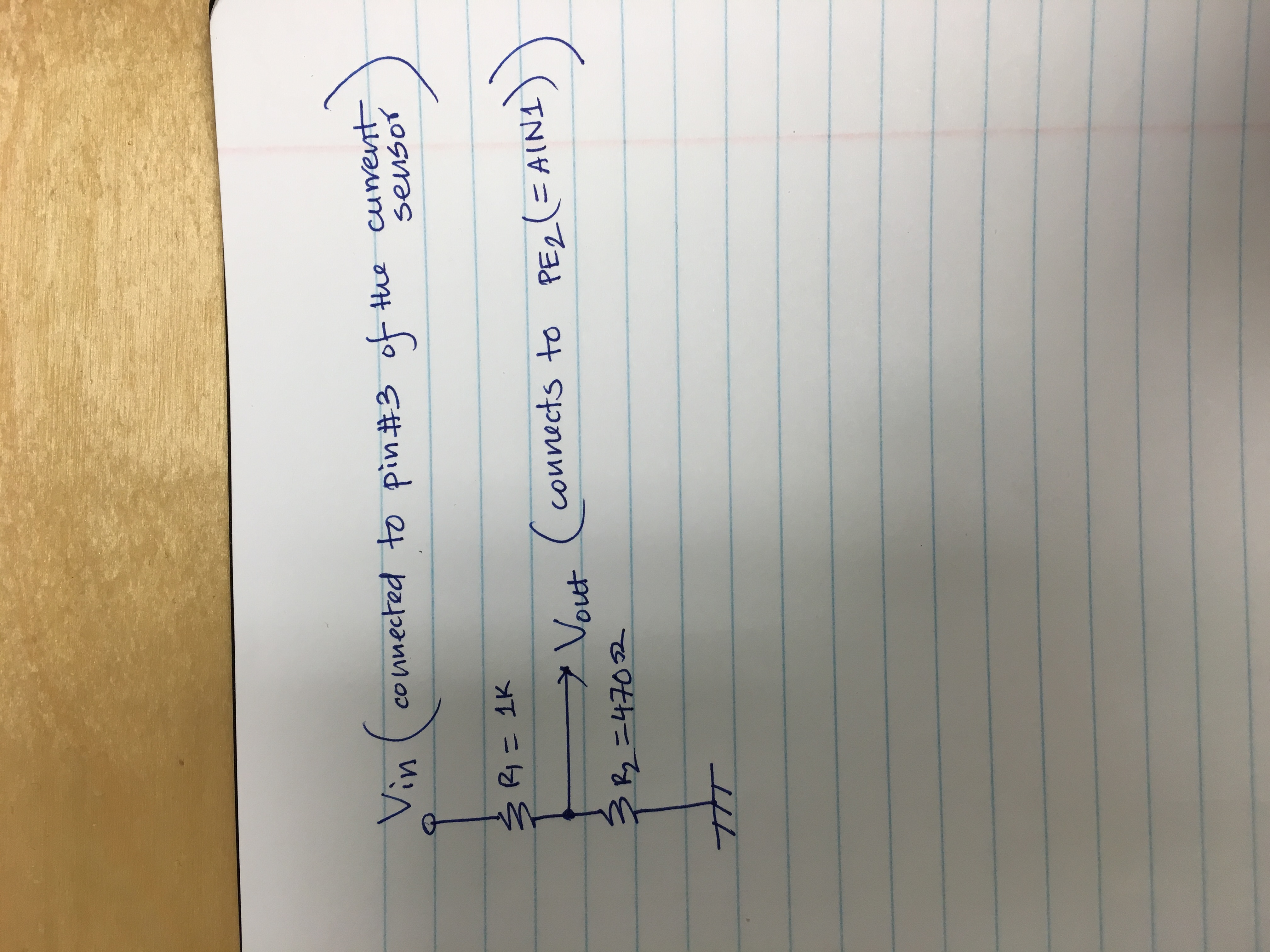
I am using the current sensor HO 10-P with my TM4C123 launchpad board. I am a bit confused how to use the sensor and read in the code. Page 12 of the datasheet has a pinmap and I am planning to use those 5 pin like below

1. Uc = supply voltage =5V

2. 0V= GND

3. Vout = it actually goes to the analog pin of the microcontroller, in this case I use A7

4. Vref = 3.3V

5. OCD = GND (as suggested by this training manual)

Having done that, I am wondering if we just read the analog pin with analogread, is that enough to find out the current value? Or do I need to do some type of mapping to extract the exact current value?

  • Hello lilyhack

    It is not clear if the output voltage is a function of Vref or the Uc. If it is the latter, then there is an issue. The pin can only read between 0 and Vdda supply of the microcontroller for ADC module.

    If it is the former case where the current equivalent voltage is between 0 and Vref, then you need to configure the GPIO as an ADC pin, configure the ADC controller to read the Vout from the sensor.

    Regards
    Amit
  • Hi Amit

    Thanks a lot for the quick reply. At page-3 of this document, I see the attached diagram. It seems Vout is a function of Vref. What do you think?


  • Hello Lily

    I would normally reconfirm with the manufacturer and set up an independent bench to validate.

    Regards
    Amit
  • Thanks Amit

    I am contacting the manufacturer, meanwhile trying to validate the assumption that Vout is a function of Vref.

    What do you mean by "you need to configure the GPIO as an ADC pin, configure the ADC controller to read the Vout from the sensor."?

    Does it mean I should connect Vout to a GPIO pin? Not to A7? And then convert that GPIO pin to an ADC pin and read?

    Can you please show a sample code snippet?
  • Hello lilyhack,

    The output of the sensor is a voltage proportional to the current being measured. This output of the sensor must be connected to a GPIO that has ADC option available on it. As an example pin PE3 is an ADC pin.

    Regards
    Amit
  • Amit

    I am a bit confused here.

    At page- 20 of this doc, it shows that PE3 is connected to GPIO. But it is not clear whether ADC option is available on that pin.

    And in this pinout diagram, it says PE3 is AIN0 but doesn't tell whether it is connected to GPIO. Also it shows PE3 as reserved. So can I use it? Or may be instead I can use PE2? 

    So how to decide on this?

  • A data sheet would be useful, your link takes me to someplace unreadable (maybe flash?)

    That said, it appears to be a relatively low current sensor family from LEM, part of the HO P series. I just had a quick glance but if I'm reading it correctly (LEM's data sheets can take several reads to be sure, they tend to the terse) the reference is a) an output not an input at about 2V5 and b) not a scale but the zero point, the signal will be below the reference for negative and above for positive current.

    I'm pretty confident in point b. The reference could also be bidirectional, possibly an input only but I don't think so.

    The voltage swing is nominally +/-2V with 1/2V headroom for overcurrent.

    You will need signal conditioning and protection as well as the usual filtering and impedance matching.

    Robert
  • Hello lilyhack,

    Please look at the datasheet of the TM4C123GH6PM device that is used on the launchpad. Also Robert raised an important point of "signal conditioning", "protection", "filtering" and "impedance matching".

    Regards
    Amit
  • Lilyhack,

    1) The sensor output is 0-5V. The ADC on TM4C123 will not convert anything above VREFA, which you will probably feed with 3.3V. So to begin with, you can't inject that voltage range into your MCU and expect it to measure. You will need signal conditioning before: voltage divider, possibly an opamp, and ideally a basic analog filter (current sensing signals tend to oscillate a lot).

    2) The Vref concept on that sensor is simply a way to offset the current range that a given sensor will be able to measure - still, the output will remain 0-5V. And the datasheet shows that 3.3V as a VREF to the SENSOR is OFF limits.

    3) To choose an input pin, look at the "Signals by Signal Name" entry of the MCU's datasheet. There are lots of analog inputs (all of the AINnn are). As for "isn't it GPIO?": almost all the pins on the MCU's are GPIO's, and the same pins have many other functions (if you haven't yet discovered that, look at the "Signals by Pin Number" and get impressed). Of course you need to write your software to configure what you want each pin to do.

    4) Don't get too crazy understanding registers and each bit of the ADC... Rather, learn to use the TivaWare ADC functions. And good luck again, trying to read electric current out of a sensor on first attempt... You will face lots of weird floating numbers before you achieve your goals...

    Bruno
  • OK, so based on the suggestion, I did below. Not sure if I am doing it right.

    How does the ADC know that I am connecting to the PE2 pin? The code doesn't seem to reflect that. What am I missing?


    1. Connected the current sensor to the TM4C123 like below

    Pin#1  Uc -> VBUS (5V)

    Pin#2 OV -> GND

    Pin#3 Vout -> Input to the voltage divider (below diagram)

    Pin#4 Vref ->3.3V

    Pin#5 OCD ->GND


    The output of the voltage divider goes to PE2 (AIN1)

    2. Code to read the sensor following Tivaware document (http://www.ti.com/lit/ug/spmu298d/spmu298d.pdf)


    void loop() {


      // Enable the ADC0 module

      SysCtlPeripheralEnable(SYSCTL_PERIPH_ADC0);


      // Wait for the ADC0 module to be ready

      while(!SysCtlPeripheralReady(SYSCTL_PERIPH_ADC0))

      {

      }


      // Enable the first sample sequencer to capture the value of channel 0 when the processor trigger occurs

      ADCSequenceConfigure(ADC0_BASE, 0, ADC_TRIGGER_PROCESSOR, 0);

      ADCSequenceStepConfigure(ADC0_BASE, 0, 0, ADC_CTL_IE | ADC_CTL_END | ADC_CTL_CH0);

      ADCSequenceEnable(ADC0_BASE, 0);


      // Trigger the sample sequence

      ADCProcessorTrigger(ADC0_BASE, 0);


      // Wait until the sample sequence has completed

      while(!ADCIntStatus(ADC0_BASE, 0, false))

      {

      }


      // Read the value from the ADC

      ADCSequenceDataGet(ADC0_BASE, 0, &ui32Value);


      Serial.print("StringCurrent=");

      Serial.println(ui32Value);     

    }


  • You're right, you need to set up the pins. The Tivaware a/d examples should show how that's done.

    The divider is a start although your max voltage is now around 1V7 centred around 0V8. You should also be adding some filtering and impedance matching. Take a search for the bookshelf tag, you will find references to TI literature on developing inputs to A/Ds

    Robert
  • Thanks Robert.

    I haven't updated the filtering yet but improving on the code side. Do you think I am good codewise?

    I followed Tivaware example in \\examples\peripherals\adc\single_ended.c and wrote below

    void loop() {
      
        // Enable the ADC0 module
        SysCtlPeripheralEnable(SYSCTL_PERIPH_ADC0);
    // For this example ADC0 is used with AIN0 on port E7 SysCtlPeripheralEnable(SYSCTL_PERIPH_GPIOE);
    // Select the analog ADC function for these pins. GPIOPinTypeADC(GPIO_PORTE_BASE, GPIO_PIN_3);
    // Enable sample sequence 3 with a processor signal trigger. ADCSequenceConfigure(ADC0_BASE, 3, ADC_TRIGGER_PROCESSOR, 0);
    // Configure step 0 on sequence 3. ADCSequenceStepConfigure(ADC0_BASE, 3, 0, ADC_CTL_CH0 | ADC_CTL_IE | ADC_CTL_END);
    // Since sample sequence 3 is now configured, it must be enabled. ADCSequenceEnable(ADC0_BASE, 3);
    // Clear the interrupt status flag. This is done to make sure the interrupt flag is cleared before we sample. ADCIntClear(ADC0_BASE, 3); while(1){ // Trigger the ADC conversion. ADCProcessorTrigger(ADC0_BASE, 3);
    // Wait for conversion to be completed. while(!ADCIntStatus(ADC0_BASE, 3, false))
    { }
    // Clear the ADC interrupt flag. ADCIntClear(ADC0_BASE, 3);
    // Read ADC Value. ADCSequenceDataGet(ADC0_BASE, 3, pui32ADC0Value);
    // Display the AIN0 (PE3) digital value on the console Serial.print("StringCurrent="); Serial.println(pui32ADC0Value[0]);
    // This function provides a means of generating a constant length delay. SysCtlDelay(SysCtlClockGet() / 12); }

    }

  • That looks approximately right, I don't have references to hand to double check but if you are following the TivaWare examples then there is a good chance that will work. All the individual pieces seem present.

    Robert