This thread has been locked.

If you have a related question, please click the "Ask a related question" button in the top right corner. The newly created question will be automatically linked to this question.

ICDI connection for custom board not working

Other Parts Discussed in Thread: TM4C1294NCPDT, TM4C123GH6PM

Hello,

I am attempting to bring up a custom board which has one TM4C1294NCPDT and one TM4C123GH6PM. I am attempting to program these devices using the 'debug out' feature of the TM4C1294 launchpad. Attempting to program either device results in a "CORTEX_M4_0: Error connecting to the target" message.

To keep things simple, I am focusing on the TM4C123 device for now. Here is what I checked so far:

  • VDD is at 3.3V, with about 100-200mV ripple observed at decoupling caps. All VDD pins are connected.
  • VDDC is at 1.2V, with about 100-200mV ripple observed at decoupling caps. This net is not shared with any other devices. All VDDC pins are connected.
  • All GND pins are connected.
  • RESETn is pulled up to 3.3V with a 10K resistor.
  • Continuity check between the following JTAG signals on target board and X1 header on the Launchpad showed a good connection: TMS, TCK, TDO, TDI, RESET, GND.
  • All resistors were removed from the X1 header on the Launchpad; R40 was removed as well.
  • Brief activity is observed on TMS, TCK, TDO, TDI on the target side when attempting to program the device. 

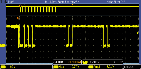
Here is what the activity on TDO looks like. Except for the first burst of activity, all subsequent bursts have the pattern seen in bursts 2 and 3. This continues for about 30 milliseconds.

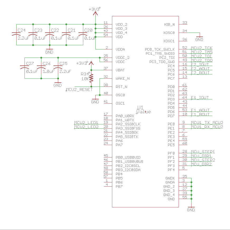
This is how the TM4C123 hardware is set up. My intention is to run the device from PIOSC.

I am using CCSv6.1.3.00033. I haven't had any problems programming TM4C chips on launchpads before, but this is the first time trying to use the 'debug out' feature.

Any suggestions on what I should investigate next?

Thanks

  • Hello,

    I recommend to add 10k pull-up resistors for TCK and TMS. The external pull-up resistors are not required if the JTAG connections are short. But if the JTAG signals are greater than 2 inches, TCK should be pulled up with a 10k resistor to prevent any transitions.

    Regards,

    QJ 

  • Hello QJ,

    I soldered 10k pull-ups from 3.3V  to TCK and TMS, but it did not help. The rise time and amount of noise on the JTAG signals looks accepatble with or without the pull-up resistors (max 1us rise, a few hundred millivolts noise), although there is quite a bit of overshoot and undershoot - as much as +/- 1V!

    The connection between the ICDI emulator and the target is simply a SAM8219-ND cable from X6 on the Launchpad to an identical header on the target board, about 1 cm from the target microcontroller. The SAM8219-ND cable is 1 foot in length, unshielded. The JTAG nets are connected directly to the target microcontoller over fairly short and straight paths. They are not connected to any loops, long traces, or test points. 

    Thanks,

    Oliver

  • Hello Oliver,

    Is the RBIAS on the TM4C1294NCPDT device on the custom board connected via RBIAS resistor?

    Regards
    Amit
  • Amit Ashara said:
    Is the RBIAS on the TM4C1294NCPDT device on the custom board connected via RBIAS resistor?

    Hi Amit,

    Might this "oft repeated" advice suggest (just maybe) that it requires, "Better Highlight" (i.e. (some) highlight) w/in the appropriate MCU & Application manuals?

    Advice - landing here - rotates quickly into forum oblivion - unlikely to be seen again.   Highlighting - multiple times/places - w/in "usual suspect" manuals/guides - (may) warrant some (slight) consideration.

  • Hello Amit,

    We did not connect an RBIAS resistor, because we are not using Ethernet on this board. As per the preferred practice (pg. 1816 of the TM4C1294NCPDT datasheet), no connection is made to the RBIAS pin. Since no external crystal is attached, we concluded that footnote 'a' should not be a problem - the ROM bootloader should not enable the Ethernet Phy.

    Thanks,
    Oliver
  • Hello Oliver,

    Can you please connect a resistor to RBIAS and check. I think the issue is still with the lack of RBIAS resistor. This will help eliminate one possible root cause.

    Regards
    Amit
  • Hello Amit,

    I managed to solder a 4.7k resistor between the RBIAS pin and ground, but I am still unable to program either the TM4C123 or the TM4C1294.

    Thanks,

    Oliver

  • Amit,

    Does the ICDI "debug out" feature require a different target configuration from the regular (internal to the Launchpad) use of the ICDI? My project(s) -- which until now exclusively used Launchpads via ICDI -- do not have target configuration files. I tried adding a target configuration file but found that the 'Test Connection' button is always unavailable.

    Thanks,
    Oliver
  • Hello Oliver,

    How have you connected the TM4C123x and TM4C129x with JTAG, is it 1 to 1 mapping or is it daisy chain of the JTAG from the header to one device, then next device and finally TDO goes back to the header?

    Regards
    Amit
  • Amit,

    It is a 1 to 1 mapping - each microcontroller has it's own pin header.
  • Hello Oliver,

    Test Connection feature is not available on the ICDI. Can you check if the TM4C123GH6PM is connecting to the ICDI?

    Regards
    Amit
  • Hello Amit,

    The TM4C123GH6PM is suffering from the same problems.

    After more testing of the board, we found that brief but large voltage spikes sometimes appear on the microcontroller's power supply rail when the board is powered on. These spikes typically only last a few hundred nanoseconds, but were as large as +8 or -4 volts. Since the board was power cycled many times (while testing other components) before we attempted to program the microcontrollers, we are investigating the possibility that the microcontrollers were damaged by repeated exposure to these power supply transients.

    The primary power supply for the board is 24 volts. A buck converter provides a 5 volt rail, and a linear regulator produces the 3.3 volt microcontroller power supply from the 5 volt rail. We used a decent amount of decoupling capacitors, but did not include include power supply filters or TVS devices. Perhaps that was a mistake. The plan for now is to install a fresh TM4C123 + supporting components on an extra PCB, and supply the linear regulator with a clean 5 volt supply (no 24 volt input will be used). We have also purchased an XDS100v2, which we will try using as soon as it arrives.

    Thanks for your help so far. I will post an update here when have completed further testing.
    Oliver
  • The XDS100v2 arrived. Here is the result of running 'Test Connection' on the initial PCB, for both the TM4C123 and the TM4C1294. 

    [Start: Texas Instruments XDS100v2 USB Debug Probe_0]
    
    Execute the command:
    
    %ccs_base%/common/uscif/dbgjtag -f %boarddatafile% -rv -o -F inform,logfile=yes -S pathlength -S integrity
    
    [Result]
    
    
    -----[Print the board config pathname(s)]------------------------------------
    
    C:\Users\LABDEV~1\AppData\Local\TEXASI~1\
        CCS\ti\0\0\BrdDat\testBoard.dat
    
    -----[Print the reset-command software log-file]-----------------------------
    
    This utility has selected a 100- or 510-class product.
    This utility will load the adapter 'jioserdesusb.dll'.
    The library build date was 'Apr 27 2016'.
    The library build time was '23:27:56'.
    The library package version is '6.0.228.0'.
    The library component version is '35.35.0.0'.
    The controller does not use a programmable FPGA.
    The controller has a version number of '4' (0x00000004).
    The controller has an insertion length of '0' (0x00000000).
    This utility will attempt to reset the controller.
    This utility has successfully reset the controller.
    
    -----[Print the reset-command hardware log-file]-----------------------------
    
    The scan-path will be reset by toggling the JTAG TRST signal.
    The controller is the FTDI FT2232 with USB interface.
    The link from controller to target is direct (without cable).
    The software is configured for FTDI FT2232 features.
    The controller cannot monitor the value on the EMU[0] pin.
    The controller cannot monitor the value on the EMU[1] pin.
    The controller cannot control the timing on output pins.
    The controller cannot control the timing on input pins.
    The scan-path link-delay has been set to exactly '0' (0x0000).
    
    -----[The log-file for the JTAG TCLK output generated from the PLL]----------
    
    There is no hardware for programming the JTAG TCLK frequency.
    
    -----[Measure the source and frequency of the final JTAG TCLKR input]--------
    
    There is no hardware for measuring the JTAG TCLK frequency.
    
    -----[Perform the standard path-length test on the JTAG IR and DR]-----------
    
    This path-length test uses blocks of 64 32-bit words.
    
    The test for the JTAG IR instruction path-length failed.
    The JTAG IR instruction scan-path is stuck-at-zero.
    
    The test for the JTAG DR bypass path-length failed.
    The JTAG DR bypass scan-path is stuck-at-zero.
    
    -----[Perform the Integrity scan-test on the JTAG IR]------------------------
    
    This test will use blocks of 64 32-bit words.
    This test will be applied just once.
    
    Do a test using 0xFFFFFFFF.
    Test 1 Word 0: scanned out 0xFFFFFFFF and scanned in 0x00000000.
    Test 1 Word 1: scanned out 0xFFFFFFFF and scanned in 0x00000000.
    Test 1 Word 2: scanned out 0xFFFFFFFF and scanned in 0x00000000.
    Test 1 Word 3: scanned out 0xFFFFFFFF and scanned in 0x00000000.
    Test 1 Word 4: scanned out 0xFFFFFFFF and scanned in 0x00000000.
    Test 1 Word 5: scanned out 0xFFFFFFFF and scanned in 0x00000000.
    Test 1 Word 6: scanned out 0xFFFFFFFF and scanned in 0x00000000.
    Test 1 Word 7: scanned out 0xFFFFFFFF and scanned in 0x00000000.
    The details of the first 8 errors have been provided.
    The utility will now report only the count of failed tests.
    Scan tests: 1, skipped: 0, failed: 1
    Do a test using 0x00000000.
    Scan tests: 2, skipped: 0, failed: 1
    Do a test using 0xFE03E0E2.
    Scan tests: 3, skipped: 0, failed: 2
    Do a test using 0x01FC1F1D.
    Scan tests: 4, skipped: 0, failed: 3
    Do a test using 0x5533CCAA.
    Scan tests: 5, skipped: 0, failed: 4
    Do a test using 0xAACC3355.
    Scan tests: 6, skipped: 0, failed: 5
    Some of the values were corrupted - 83.3 percent.
    
    The JTAG IR Integrity scan-test has failed.
    
    -----[Perform the Integrity scan-test on the JTAG DR]------------------------
    
    This test will use blocks of 64 32-bit words.
    This test will be applied just once.
    
    Do a test using 0xFFFFFFFF.
    Test 1 Word 0: scanned out 0xFFFFFFFF and scanned in 0x00000000.
    Test 1 Word 1: scanned out 0xFFFFFFFF and scanned in 0x00000000.
    Test 1 Word 2: scanned out 0xFFFFFFFF and scanned in 0x00000000.
    Test 1 Word 3: scanned out 0xFFFFFFFF and scanned in 0x00000000.
    Test 1 Word 4: scanned out 0xFFFFFFFF and scanned in 0x00000000.
    Test 1 Word 5: scanned out 0xFFFFFFFF and scanned in 0x00000000.
    Test 1 Word 6: scanned out 0xFFFFFFFF and scanned in 0x00000000.
    Test 1 Word 7: scanned out 0xFFFFFFFF and scanned in 0x00000000.
    The details of the first 8 errors have been provided.
    The utility will now report only the count of failed tests.
    Scan tests: 1, skipped: 0, failed: 1
    Do a test using 0x00000000.
    Scan tests: 2, skipped: 0, failed: 1
    Do a test using 0xFE03E0E2.
    Scan tests: 3, skipped: 0, failed: 2
    Do a test using 0x01FC1F1D.
    Scan tests: 4, skipped: 0, failed: 3
    Do a test using 0x5533CCAA.
    Scan tests: 5, skipped: 0, failed: 4
    Do a test using 0xAACC3355.
    Scan tests: 6, skipped: 0, failed: 5
    Some of the values were corrupted - 83.3 percent.
    
    The JTAG DR Integrity scan-test has failed.
    
    [End: Texas Instruments XDS100v2 USB Debug Probe_0]
    

    [Start: Texas Instruments XDS100v2 USB Debug Probe_0]
    
    Execute the command:
    
    %ccs_base%/common/uscif/dbgjtag -f %boarddatafile% -rv -o -F inform,logfile=yes -S pathlength -S integrity
    
    [Result]
    
    
    -----[Print the board config pathname(s)]------------------------------------
    
    C:\Users\LABDEV~1\AppData\Local\TEXASI~1\
        CCS\ti\0\0\BrdDat\testBoard.dat
    
    -----[Print the reset-command software log-file]-----------------------------
    
    This utility has selected a 100- or 510-class product.
    This utility will load the adapter 'jioserdesusb.dll'.
    The library build date was 'Apr 27 2016'.
    The library build time was '23:27:56'.
    The library package version is '6.0.228.0'.
    The library component version is '35.35.0.0'.
    The controller does not use a programmable FPGA.
    The controller has a version number of '4' (0x00000004).
    The controller has an insertion length of '0' (0x00000000).
    This utility will attempt to reset the controller.
    This utility has successfully reset the controller.
    
    -----[Print the reset-command hardware log-file]-----------------------------
    
    The scan-path will be reset by toggling the JTAG TRST signal.
    The controller is the FTDI FT2232 with USB interface.
    The link from controller to target is direct (without cable).
    The software is configured for FTDI FT2232 features.
    The controller cannot monitor the value on the EMU[0] pin.
    The controller cannot monitor the value on the EMU[1] pin.
    The controller cannot control the timing on output pins.
    The controller cannot control the timing on input pins.
    The scan-path link-delay has been set to exactly '0' (0x0000).
    
    -----[The log-file for the JTAG TCLK output generated from the PLL]----------
    
    There is no hardware for programming the JTAG TCLK frequency.
    
    -----[Measure the source and frequency of the final JTAG TCLKR input]--------
    
    There is no hardware for measuring the JTAG TCLK frequency.
    
    -----[Perform the standard path-length test on the JTAG IR and DR]-----------
    
    This path-length test uses blocks of 64 32-bit words.
    
    The test for the JTAG IR instruction path-length failed.
    The JTAG IR instruction scan-path is stuck-at-ones.
    
    The test for the JTAG DR bypass path-length failed.
    The JTAG DR bypass scan-path is stuck-at-ones.
    
    -----[Perform the Integrity scan-test on the JTAG IR]------------------------
    
    This test will use blocks of 64 32-bit words.
    This test will be applied just once.
    
    Do a test using 0xFFFFFFFF.
    Scan tests: 1, skipped: 0, failed: 0
    Do a test using 0x00000000.
    Test 2 Word 0: scanned out 0x00000000 and scanned in 0xFFFFFFFF.
    Test 2 Word 1: scanned out 0x00000000 and scanned in 0xFFFFFFFF.
    Test 2 Word 2: scanned out 0x00000000 and scanned in 0xFFFFFFFF.
    Test 2 Word 3: scanned out 0x00000000 and scanned in 0xFFFFFFFF.
    Test 2 Word 4: scanned out 0x00000000 and scanned in 0xFFFFFFFF.
    Test 2 Word 5: scanned out 0x00000000 and scanned in 0xFFFFFFFF.
    Test 2 Word 6: scanned out 0x00000000 and scanned in 0xFFFFFFFF.
    Test 2 Word 7: scanned out 0x00000000 and scanned in 0xFFFFFFFF.
    The details of the first 8 errors have been provided.
    The utility will now report only the count of failed tests.
    Scan tests: 2, skipped: 0, failed: 1
    Do a test using 0xFE03E0E2.
    Scan tests: 3, skipped: 0, failed: 2
    Do a test using 0x01FC1F1D.
    Scan tests: 4, skipped: 0, failed: 3
    Do a test using 0x5533CCAA.
    Scan tests: 5, skipped: 0, failed: 4
    Do a test using 0xAACC3355.
    Scan tests: 6, skipped: 0, failed: 5
    Some of the values were corrupted - 83.3 percent.
    
    The JTAG IR Integrity scan-test has failed.
    
    -----[Perform the Integrity scan-test on the JTAG DR]------------------------
    
    This test will use blocks of 64 32-bit words.
    This test will be applied just once.
    
    Do a test using 0xFFFFFFFF.
    Scan tests: 1, skipped: 0, failed: 0
    Do a test using 0x00000000.
    Test 2 Word 0: scanned out 0x00000000 and scanned in 0xFFFFFFFF.
    Test 2 Word 1: scanned out 0x00000000 and scanned in 0xFFFFFFFF.
    Test 2 Word 2: scanned out 0x00000000 and scanned in 0xFFFFFFFF.
    Test 2 Word 3: scanned out 0x00000000 and scanned in 0xFFFFFFFF.
    Test 2 Word 4: scanned out 0x00000000 and scanned in 0xFFFFFFFF.
    Test 2 Word 5: scanned out 0x00000000 and scanned in 0xFFFFFFFF.
    Test 2 Word 6: scanned out 0x00000000 and scanned in 0xFFFFFFFF.
    Test 2 Word 7: scanned out 0x00000000 and scanned in 0xFFFFFFFF.
    The details of the first 8 errors have been provided.
    The utility will now report only the count of failed tests.
    Scan tests: 2, skipped: 0, failed: 1
    Do a test using 0xFE03E0E2.
    Scan tests: 3, skipped: 0, failed: 2
    Do a test using 0x01FC1F1D.
    Scan tests: 4, skipped: 0, failed: 3
    Do a test using 0x5533CCAA.
    Scan tests: 5, skipped: 0, failed: 4
    Do a test using 0xAACC3355.
    Scan tests: 6, skipped: 0, failed: 5
    Some of the values were corrupted - 83.3 percent.
    
    The JTAG DR Integrity scan-test has failed.
    
    [End: Texas Instruments XDS100v2 USB Debug Probe_0]
    

  • Hello Oliver,

    Test Connection shows that the JTAG chain is not complete. This I have only seen when the JTAG interface is not correctly done or if there is a mismatch in the configuration (ccxml: make sure return TCK/adapative clocking is not selected) or if the device is not powered.

    I would request the schematic of TM4C123GH6PM and the JTAG header. Also which XDS100v2 header are you using, ARM-10, ARM-20, CTI-20, etc.

    Regards
    Amit
  • Amit,

    We are using the ARM-10 header on both the XDS100 and the target board.

    I have attached a screen capture of the schematic for the TM4C123GH6PM and it's JTAG header. Let me know if you need a more complete schematic; I will need to check on legal restrictions.

    We neglected the VTARGET connection for pin 1, since the design was based on (and intended for use with) the Launchpad ICDI circuit. However, we can easily make this connection manually between the 20-pin header of the XDS100 and a test point for the 3.3V supply on the target board. 

    Thanks again,

    Oliver

  • Hello Oliver,

    You are using ARM10-pin header but referring to 20 pin header on the XDS100. Do you intent to wire the JTAG manually?

    I would suggest soldering a wire for Vtref.

    Regards
    Amit
  • Off topic, but I just want to add that I was also caught out by the missing RBIAs resistor. Like others I followed the advice. I have contacted TI and they have no intention of correcting the silicon error. (BTW, the preproduction samples worked fine!). Time for the documentation to be updated I think.
  • Hello Vito

    In this case we have already eliminated the RBIAS. The issue is more generic on the JTAG interface.

    This is not a silicon error, but datasheet error where the acceptable practice of NA has been put. If a PHY enabled part is used, then the ROM boot loader expects PHY to be operational for Ethernet Boot Loader.

    Regards
    Amit
  • Amit,

    I am using the ARM 10-pin header on the XDS100 and the target board for the core JTAG signals (TCK, TMS, TDO, TDI) and GND. They are connected with the standard cable provided in the XDS100 kit: Samtec FFSD-05-D

    I only mentioned the 20-pin header to say that there is an easy way to provide VTARGET to the XDS100 without further modifying the target board.

    Thanks,

    Oliver

  • Hello Oliver

    Or you can run a small wire on the main board.

    Regards
    Amit