This thread has been locked.

If you have a related question, please click the "Ask a related question" button in the top right corner. The newly created question will be automatically linked to this question.

Does DIVSCLK set as SYSCLK derived MOSC source remain synchronous to System Clock and how 2 make DIVSCLK & RTCCLK external pins work?

Guru 55913 points
Other Parts Discussed in Thread: EK-TM4C1294XL

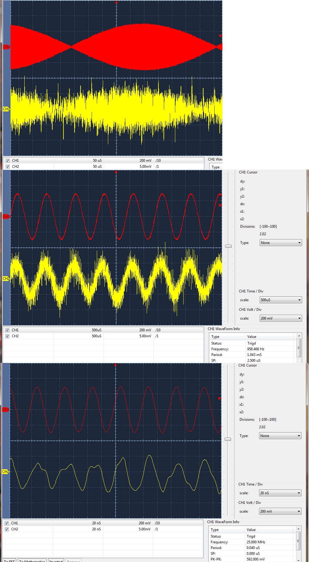
Is not SYSCLK an acronym of System Clock and would SYSCLK not be synchronous to its own time base when set to DIVSCLK?

Main clock tree only shows gated logic in the path between MOSC and DIVSCLK.

Would like to experiment synchronize (4) TM4C1294 using single MOSC XTAL source and make 3 additional MCU driven by DIVSCLK. Will the DIVSCLK driven PLL's synchronize to the single primary MOSC?

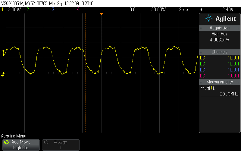
Optional Clock Output Signal (DIVSCLK):
An optional clock output, DIVSCLK, is provided which can be used as a clock source to an external
device but bears no timing relationship to other signals. Note that this signal is not synchronized to
the System Clock. By programming the SRC field in the Divisor and Source Clock Configuration
(DIVSCLK) register, the following clock outputs may be selected for DIVSCLK:
■ System Clock
■ PIOSC
■ MOSC

  • Hello BP101

    Yes, SYSCLK is an acronym for System Clock

    The DIVSCLK is synchronous to the source that has been used to generate the same as per the register setting in DIVSCLK register of the system control module. There would be path delay, so there may be a phase difference on a part-to-part basis.

    Regards
    Amit
  • Hi Amit,

    Odd way to state GPIO propagation path delay, data sheet text simply stating "DIVSCLK is not synchronous." Seemingly slave pears PLL locking around clock jitter from DIVSCLK phase difference to a masters MOSC might be insignificant. Concerning are slave mirrored peripherals that would further divide masters MOSC driven SYSCLK being used to clock each slave peripheral synchronous to the masters 480Mhz PLL and 25Mhz MOSC.

    Goal is to gain dedicated master/slave mirrored peripheral load balancing capability in specific peripherals such a PWM.

    Simply put all slaves MOSC are then driven by the masters DIVSCLK and all slaves PLL's seemingly would be synchronous to each other. 

    The question is how much phase shift propagation delay is expected masters MOSC porting into DIVSCLK and slaves SYSCLK difference?

    Is there an undocumented Min/Max electrical characteristic for the phase shift and or DIVSCLK propagation delay or any TI Wiki notes for master/slave MCU?

  • Hello BP101

    The DIVSCLk clock source can be different from the system clock as stated earlier. Also since it is a clock out, the path delay would be different on part to part as delay buffers are there on the path which have a PVT dependency. So by stating that the clock will always be in phase and frequency with the source clock would be an incorrect statement
  • Hi Amit,

    >So by stating that the clock will always be in phase and frequency with the source clock would be an incorrect statement.

    Where in the clock tree (Fig5-5) are said (buffers) illustrated in the path out to DIVSCLK and how is that any different from SYSCLK gating paths in each peripherals clock gating? Your answer does not indicate how much phase delay could be expected (Min/Max) in that buffer path or any percent of MCU's tested. Seems DIVSCLK is perhaps useless for synchronous I/O bus operations of the master MCU and was never tested as a slave clock source to parallel MCU together.

    >delay buffers are there on the path which have a PVT dependency.
    Please elaborate what is PVT dependency? ( Parallel variable time)

    Seems like from your answers it might be better to use an external oscillator and feed all parallel processors from the same clock source. The question then remains will all parallel MCU PLL's lock synchronous to a single clock source???
  • Hello BP101

    The functional clock tree diagram in the data sheet does not show buffers, if that is what you meant. In fact no vendor/manufacturer does that (or atleast my read of competitor data sheets don't show any such information).

    We do not quantify the Min-Max as it is stated by data sheet to be asynchronous

    PVT stands for process, voltage and temperature.

    A single crystal connected to a Clock Distribution chip can do the trick. But power up may be at slightly different times, meaning they could still be out of sync.
  • And would not the output of multiple PLLs be out of sync even with a slaved master clock and the same startup time?

    Robert
  • Hello Robert

    Yes, it would too.
  • Hi Amit,

    DIVSCLK is Asynchronous?

    >But power up may be at slightly different times, meaning they could still be out of sync.

    Are you are referring to each MCU's peripheral time bases out of sync or the point at which each POR MCU enters the stand by state?

    Seemingly PLL of each MCU should lock onto the provided input frequency of the single clock source, that is unless the PLL high pass filter phase angle is unstable and or unpredictable. That would seem unlikely given COG ceramic capacitor filters are highly precise, have low little frequency drift and are extremely temperature stable.

  • Hello BP101,

    I am referring to the time when each of the MCU comes out of the power on state and begins its execution.
  • Thanks Amit, I thought that should be the case but I wasn't sure.

    Robert
  • Hi Amit,

    Interestingly it would seem digital capacitor tuning TM4C PLL high pass filter would be extremely precise locking frequency to MOSC. Seemingly all MCU's would at some point synchronize  480Mhz VCO after POR and clock cool off.  Have past encountered VCO frequency multiplication in 14 pin dip CMOS PLL,  used decade counters for the multiplication of VCO's low pass filter yet nothing close to 480Mhz but recall the input frequency lock of VCO filter could be tweaked by the digital capacitor value.

    Curious to see DIVSCLK output can not get working EK-TM4C1294NCDTi3-XL using only possible port Q pin 4, out X11-pin 93.

    Can't find a configuration call GPIOPinTypeDivsclk() and set HW direction versus OUT, but how to select the digital pin 7 ??

    /* Enable 25Mhz MOSC clock output as DIVSCLK on PQ4 pin 102 */
    ROM_SysCtlClockOutConfig(SYSCTL_DIVSCLK_SRC_MOSC | SYSCTL_DIVSCLK_EN, 1);
    
    //********************************************************
    // DIVSCLK = MOSC 25Mhz: GPIO PQ4 pin 102
    // TM4C1294LP: X11-Pin93
    
    MAP_GPIOPadConfigSet(GPIO_PORTQ0_AHB_BASE, GPIO_PIN_4, GPIO_STRENGTH_2MA, GPIO_PIN_TYPE_STD);
    MAP_GPIODirModeSet(GPIO_PORTQ0_AHB_BASE, GPIO_PIN_4, GPIO_DIR_MODE_HW);


  • Hello BP101

    It seems you forgot the configuration of PCTL.... Following is a working configuration

    MAP_GPIOPinConfigure(GPIO_PQ4_DIVSCLK);
    GPIODirModeSet(GPIO_PORTQ_BASE, GPIO_PIN_4, GPIO_DIR_MODE_HW);
    GPIOPadConfigSet(GPIO_PORTQ_BASE, GPIO_PIN_4, GPIO_STRENGTH_2MA, GPIO_PIN_TYPE_STD);
  • Hi Amit,

    Adding the PCTL command caused odd looping just after reset and MOS clock setup. Moving DIVSCLK APP setup further out beyond MOSC clock setup stopped looping, yet still no signal PQ4. There is a 1 second SysCtlDelay after MOSC clock setup and oddly even that cool down didn't stop DIVSCLK setup from looping.
  • Hello BP101,

    PCTL is a mux control, so there is no looping involved.
  • Hi Amit,

    Seemingly it was the DIVSCLK application configuration and linear proximity to MOSC clock configuration that caused looping resets but only after PCTL was configured. All looping stopped after moving DIVSCLK away from the MOSC clock configuration.

    The DIVSCLK signal X11-Pin93 is only 200mv peak but only in various places in wave form and the frequency is moving all over, 4.5Mhz up to 25Mhz.

    Does that DIVSCLK wave form behavior sound correct?
  • Hello BP101

    No, it does not seem right. Check the scope setting and time base. I am using it to generate 8MHz to 24Mhz clocks without issues.
  • Hi Amit,

    The scope is 30Mhz 10K samples depth 50mv/cm^2, channel set for x10 probe yet the frequency is not stable. Was expecting DIVSCLK amplitude close to TTL level being driven by GPIO port set 2ma drive strength. Seems there is something wrong in the DIVCLK configuration?

  • Hello BP101

    And AC or DC bias. Did you try other settings for the Divided clock?
  • Hi Amit,

    Good points - adding WPU or set the divisor 4 makes no difference to output frequency or amplitude remain the same.

    Must be the GPIO MUX digital 7 (DIVSCLK) PQ4 is not actually being configured? The port configurations are right in the middle of other ports proven as being configured. There are only 2 digital selections 1 & 7 on PQ4 and digital 1=U1RX.
  • Hello BP101

    Debug.... Check the PCTL, AFSEL, DEN and ODR values.
  • Hi Amit,

    Seems the simple is not so simple in the PCTL both DIVSCLK and RTCCLK  produce similar distorted wave forms.

    May also need non interrupted 60hz RTC time base for the fan speed taco RPM formula.  Oddly GPTM edge counter and GPTM 60hz timers slowly become diverged when PWM output is more time predominate during BLDC motor acceleration. So the fan speed edge counts and RPM climbs with the BLDC motor speed. Even more strange It don't matter much the interrupt priority of GPTM's, both are set 0x40/IRQ51,36 just below PWM counter reloads IRQ27/0x20 higher priority and ADC SSIO's etc.... Tried some trickery to 1sec GPTM periodic and set 5ms time then incremented variable++ to % in 1 sec interval inside interrupt hander yet same thing occurs.

    The fan speed edge taco RPM at idle mode works great and will measure 600-6300 RPM via CCP PWM duty cycle changes.  The GPTM RTC mode might be the cure if can get it working and did insure the Hibernate peripheral is enabled..

    //********************************************************
    // RTCCLK = RTOSC 32.768 KHz: GPIO PP3 pin 104
    // TM4C1294LP: BP2-X7-16, X11-Pin73
    
    MAP_GPIOPinConfigure(GPIO_PP3_RTCCLK);
    MAP_GPIODirModeSet(GPIO_PORTP0_AHB_BASE, GPIO_PIN_3, GPIO_DIR_MODE_HW);
    MAP_GPIOPadConfigSet(GPIO_PORTP0_AHB_BASE, GPIO_PIN_3, GPIO_STRENGTH_2MA, GPIO_PIN_TYPE_STD);

  • Hello BP101

    I should be able to give you a simple code for the EK-TM4C1294XL which shows how to get the DIVSCLK next week....
  • Hi Amit,

    That DIVSCLK example would be great. Perhaps something odd is up with GPIO external clocking MUX selections. Hibernate module required more configuration (below) to witness debug RTC counter 1 sec intervals occurring. Yet still can not see 32kHz on GPIO pin PP3 either with STD or OD as debug 0xC or 0x8 for PP3.

    Is that PCTL/PMC3=0x00007000 decode correct bit pattern for RTC on PP3?

        /* Enable the system clock for Hib module */
    	ROM_HibernateEnableExpClk(g_ui32SysClock);
    	// Delay 3 SYSCLKS/25ns for Hib module to stabelize.
    	ROM_SysCtlDelay(6);
    	/* Set the Hibernate XTAL capacitors for 12pf */
    	ROM_HibernateClockConfig(HIBERNATE_OSC_LOWDRIVE);
        /* Enable the Real Time clock RTCCK */
    	ROM_HibernateRTCEnable();

  • Hello BP101

    GPIOODR for the corresponding pin must be 0 and not 1 as per the snapshot image of the GPIO Port P Pin-3
  • Hi Amit,

    >GPIOODR for the corresponding pin must be 0 and not 1 as per the snapshot image of the GPIO Port P Pin-3

    RTCCLK is on pin (PP3/0x8) and pin DIR you see is another configured GPIO pin (PP2/0x4) but also tested both PP3/PQ4 as OD. Good thing I enabled RTC as it has revealed some more oddness in DIVSCLK and RTCCLK.

    Oddly both external pins DIVSCLK, RTCCLK PCTL decodes = (7). Dividing 25Mhz MOS DIVSCLK % 4 = 25kHZ ?? on PQ4 after configuring 32Khz RTCCLK.

    CH1= PP3 RTC frequency ?? and CH2=PQ4 DIVSCLK%4=25Khz ....  Something possibly not correct in the PCTL decodes??

    Debug GPIO of PQ4 :


  • Hi Amit,

    It seems DIVSCLK may be configured properly after all but still not working. Oddly Y3 - 32kHz HIB clock appears stable yet may be injecting 830-870Hz harmonics into MOSC some where along the clock tree chain.  These two LP are recent purchased EK-TM4C1294NCPDTi3-XL few months ago.

    Have discovered MOSC has 958Hz harmonics (top/center) captures show sine wave riding Y1 25Mhz frequency (CH1).

    Oddly when X10 scope probe (CH1) is place one side of C44 the 25Mhz MOSC output to DIVSCLK (CH2) frequency occurs yet is distorted with harmonic noise, (bottom) capture. The scope then captures 25Mhz but the MOSC frequency is very unstable. Hard to imagine 480Mhz PLL being any where close to stable in this scenario let alone PLL actually locking if this harmonic 2nd fundamental frequency is present.   

  • Hello BP101

    Oddly, I have not seen such interference. But glad to hear that it is now working on the pins as expected by the data sheet.
  • Hi Amit,

    Seems you have missed the point that  Y1 is not oscillating correctly and seemingly has 830-870hz harmonics.  Holding scope probe on C44 makes the DIVSCLK then produce a 25Mhz MOSC yet still produces those unstable harmonics. Otherwise DIVSCLK is a highly chaotic signal wave form removing the scope probe from C24 C44.

    According to LP schematic C44/45 should be 12pf. Question is might the MOSC clock configuration have some issue causing the Y1 behave badly?

    Current clock configuration: With or without 1st line HWREG, the same harmonic is present.

    HWREG(SYSCTL_MOSCCTL) |= SYSCTL_MOSC_HIGHFREQ;
    
    g_ui32SysClock = MAP_SysCtlClockFreqSet((SYSCTL_XTAL_25MHZ |
                                              SYSCTL_OSC_MAIN |
                                              SYSCTL_USE_PLL |
                                              SYSCTL_CFG_VCO_480), 120000000);

  • Hello BP101

    Attached is a simplified project which configures the DIVSCLK and the associated snapshot of the clock capture on a scope.

    tm4c1294_divsclk.zip

    The clock is not a perfect square or sine, with some reflections evident (but nothing in the Hz range). Since, there is not much I can do other than provide any reference data, I can consider the post closed with proof of code and observations.

  • Hi Amit,

    The first MOSC capture provided above certainly does not represent a properly running oscillator when being chopped by low frequency.

    Thanks for DIVSCLK and simply renamed debug (main.obj) to (main.bin) flashed LP and will not initialize MOSC. Project import fails with error latest 5.2.7 or 16.3.0 compilers.
  • Hi Amit,

    The story gets worse when Initializing MOSC datasheet 5.3 and clearing REG 10 MOSCCTL, RW bit 2 NOXTAL kills the TM4C1294NCPDTi3. LMF build 1613 will unlock target yet can no longer initialize target 0.

    NOXTAL Bit 2: RESET=1

    This bit should be cleared when a crystal or oscillator is connected to the OSC0 and OSC1 inputs, regardless of whether or not the MOSC is used or powered down. Note: For proper clock functionality when switching to crystal mode, software must clear this bit and set the PWRDN bit in a single write access.

    MOSC initialization routine that finally killed the newer launch pad:

    	 /* Set the MOSC for High frequency oscillator */
    	 HWREG(SYSCTL_MOSCCTL) |= SYSCTL_MOSC_HIGHFREQ;
    	 /* When an attached crystal clear PWRDWN and NOXTAL bits */
    	 HWREG(SYSCTL_MOSCCTL) &= ~(SYSCTL_MOSC_PWR_DIS | SYSCTL_MOSC_NO_XTAL);
    	 /* Wait until the MOSC indicates fully powered up */
    	 while((!HWREG(SYSCTL_RIS) & SYSCTL_INT_MOSC_PUP))
    	 {
    	 }
    	

  • The launch pad MOSC is perpetually locked after following the directions to clear the NOXTAL bit for the presence of an external crystal. Unlocking the DAP does NOT restore TM4C1294 Launch Pad to an unlocked and running condition.

    Note: This bit should be cleared when a crystal or oscillator is connected to the OSC0 and OSC1 inputs, regardless of whether or not the MOSC is used or powered down. For proper clock functionality when switching to crystal mode, software must clear this bit and set the PWRDN bit in a single write access.
  • Hello BP101

    I guess this is another thread....
  • Hi Amit,

    Seems this thread DIVSCLK has underlying MOSC oscillator issues. Not so happy thus programmatically have Killed a new launch pad in the process of trying to make 25Mhz MOSC oscillate without so much secondary fundamental harmonics.

    It's amazing the PLL locks to this very wavy wave form.