


I'm not sure if this forum accepts PCB/schematic design question, but I will move my question over to another forum if needed.
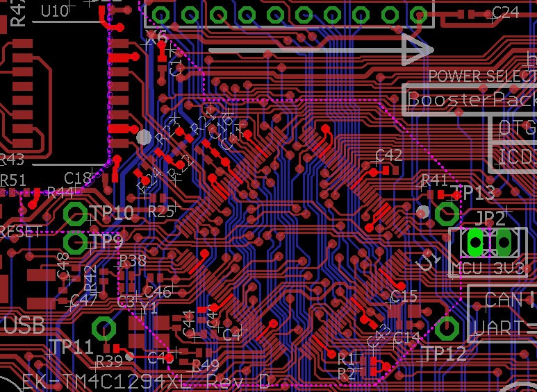
I'm trying to learn how to do PCB design, and I thought that it would be best to take a look at the schematic and board files for the current launchpad that I'm working with. When I'm trying to see how power is being supplied to the MCU, I'm having a hard time tracing back from where power is entering (either through IDCI or OTG USB port) to where power should be going to (the VDD pins on the MCU). They seem to be leading to this part U4, which is a power-distribution switch, but then it goes off to some other places from there, and not to any of the VDD pins on the MCU. There is a pin from the switch that leads to all of the booster packs' and GPIO breakout holes, but that's to supply power to other peripherals, so not really what I'm looking for.


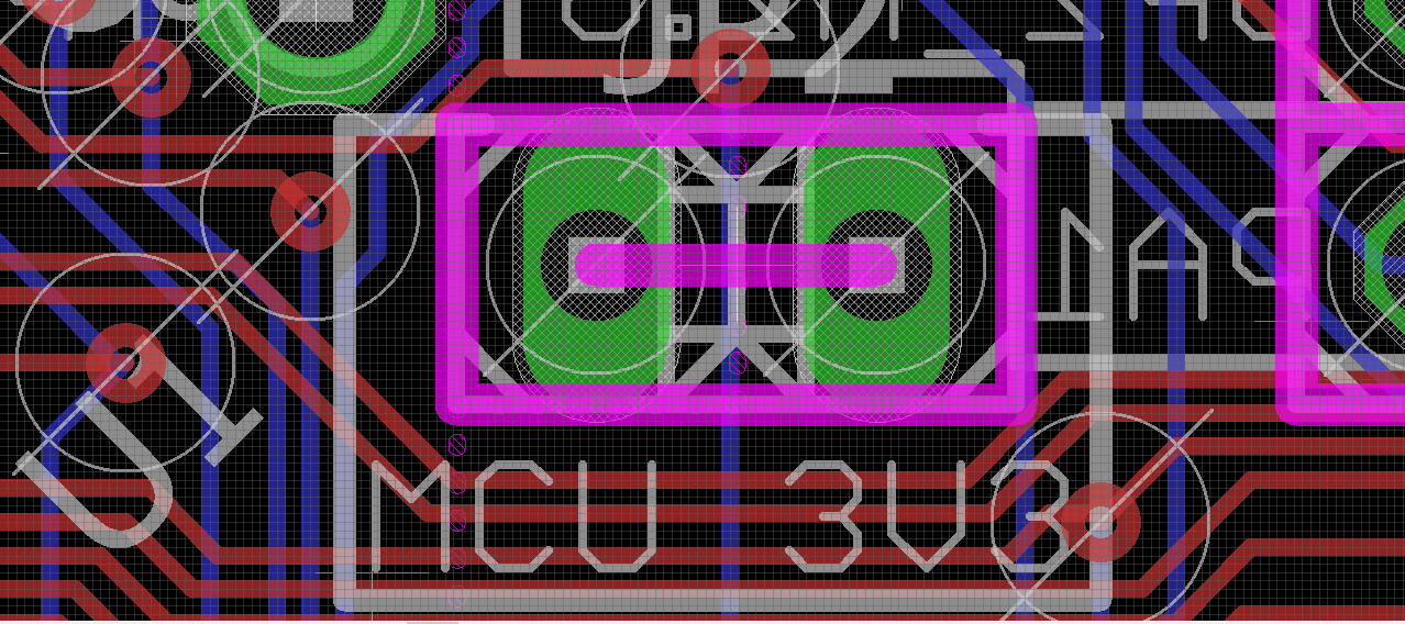
The next two pictures show the VDD lines for the MCU, as well as a jumper that is named "MCU 3.3V". It lights up together with the VDD lines when I select VDD, but I don't see anything leading to or from it. What is it there for?
Thanks
