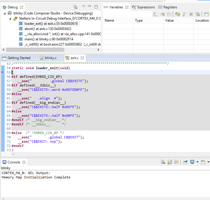
Hi All,
I'm trying to use the SSI2 module (PB4-7) to talk to the MCP3008 ADC peripheral via Freescale SPI. I am using the Keil Compiler/IDE. I used this youtube video to give me some guidance on how to set everything as well as the instructions from the datasheet (copied into my comments).
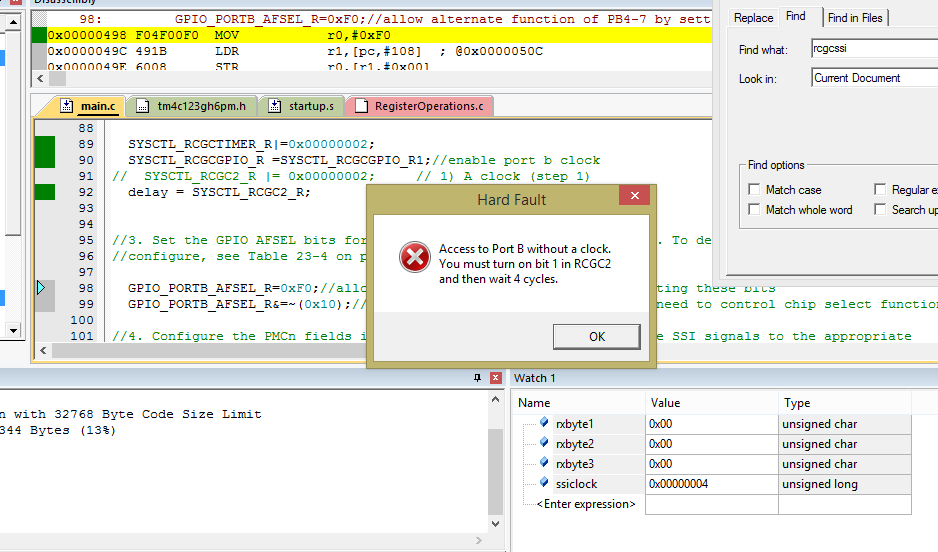
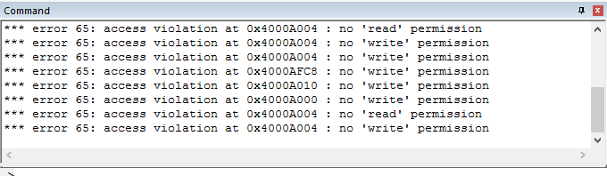
However, when I try to set up all the SSI registers in a debug session, certain ones exhibit error 65: no read/write permission seen here:
I followed the instructions exactly when writing the code (see below) as the datasheet said so I'm a bit confused as to what the problem could be. Any tips?
void SSI2_Init(void){ volatile unsigned long delay;
//For this example going to set up PB4-7 as Clock, FSS (Slave Select), RX, and TX respectively
//Initialization and Configuration
//To enable and initialize the SSI, the following steps are necessary:
//1. Enable the SSI module using the RCGCSSI register (see page 344).
SYSCTL_RCGCSSI_R=0x04;//Set bit 2 of RCGCSSI register, thus enabling Port B/Module 2 as an SSI port
Delay();
//2. Enable the clock to the appropriate GPIO module via the RCGCGPIO register (see page 338).
//To find out which GPIO port to enable, refer to Table 23-5 on page 1344.
SYSCTL_RCGC2_R |= 0x00000002; // 1) A clock (step 1)
delay = SYSCTL_RCGC2_R;
//3. Set the GPIO AFSEL bits for the appropriate pins (see page 668). To determine which GPIOs to
//configure, see Table 23-4 on page 1337.
GPIO_PORTB_AFSEL_R=0xF0;//allow alternate function of PB4-7 by setting these bits
GPIO_PORTB_AFSEL_R&=~(0x10);//****turn off AFSEL for PB5 since we need to control chip select functionality
//4. Configure the PMCn fields in the GPIOPCTL register to assign the SSI signals to the appropriate
//pins. See page 685 and Table 23-5 on page 1344.
//First go to page 1344, see that we need a value of 2 for each of the bitfields of PB4-7
GPIO_PORTB_PCTL_R =0x22220000;
///////////////PICK UP HEREEEEE youtu.be/VprofC5ssi4
//5. Program the GPIODEN register to enable the pin's digital function. In addition, the drive strength,
//drain select and pull-up/pull-down functions must be configured. Refer to “General-Purpose
//Input/Outputs (GPIOs)” on page 649 for more information.
//Note: Pull-ups can be used to avoid unnecessary toggles on the SSI pins, which can take the
//slave to a wrong state. In addition, if the SSIClk signal is programmed to steady state
//High through the SPO bit in the SSICR0 register, then software must also configure the
//GPIO port pin corresponding to the SSInClk signal as a pull-up in the GPIO Pull-Up
//Select (GPIOPUR) register.
GPIO_PORTB_DEN_R=0xF0; //enable digital for PB4-7
GPIO_PORTB_DIR_R=0x10;//make PB5 an output
//For each of the frame formats, the SSI is configured using the following steps:
//1. Ensure that the SSE bit in the SSICR1 register is clear before making any configuration changes.
SSI2_CR1_R&=0xD; //clear bit 1 (SSE bit) of the SSI2 Control Register 1
//^^^error 65: access violation at 0x4000A004: no 'read' permission
//2. Select whether the SSI is a master or slave:
//a. For master operations, set the SSICR1 register to 0x0000.0000
//b. For slave mode (output enabled), set the SSICR1 register to 0x0000.0004.
//c. For slave mode (output disabled), set the SSICR1 register to 0x0000.000C.
SSI2_CR1_R=0x00000000;//configure for master mode
//^^error 65: access violation at 0x4000A004: no 'write' permission
//3. Configure the SSI clock source by writing to the SSICC register.
SSI2_CC_R=0x0;//use system clock with divisor factor enabled
//error 65: access violation at 0x4000AFC8: no 'write' permission
//4. Configure the clock prescale divisor by writing the SSICPSR register.
//SSInClk = SysClk / (CPSDVSR * (1 + SCR))
SSI2_CPSR_R=0x08;//set prescaler for clock (assuming system clock is 16MHz) to start, scale down to 2MHz
//5. Write the SSICR0 register with the following configuration:
//¦ Serial clock rate (SCR)
//¦ Desired clock phase/polarity, if using Freescale SPI mode (SPH and SPO)
//¦ The protocol mode: Freescale SPI, TI SSF, MICROWIRE (FRF)
//¦ The data size (DSS)
//15:8 SCR prescaler
//Want this set to 0 (no additional scaling): 0x00
//7 SPH (Serial Clock Phase) 0 captures on rising edge, 1 captures on falling edge
//want to capture on rising edge
//6 SPO (Serial Clock Polarity) 0 is idle low, 1 is idle high
//want idle low clock
//Want to run in 0,0 mode (capture rising edge, idle low)
//5:4 SSI Frame Format Select 0x0=Freescale SPI, 0x1=TI Protocol, 0x2=Microwire protocol
//3:0 data select size
//want 8 bit size since we will need to send 3 bytes (24 bits) during each transaction
SSI2_CR0_R=0x07; // all bits cleared except data size for 8 bits
//6. Optionally, configure the SSI module for µDMA use with the following steps:
//a. Configure a µDMA for SSI use. See “Micro Direct Memory Access (µDMA)” on page 585 for
//more information.
//b. Enable the SSI Module's TX FIFO or RX FIFO by setting the TXDMAE or RXDMAE bit in the
//SSIDMACTL register.
//*****Don't use for now but reevaluate whether I should when I start using interrupts****///
//7. Enable the SSI by setting the SSE bit in the SSICR1 register.
//As an example, assume the SSI must be configured to operate with the following parameters:
//¦ Master operation
//¦ Freescale SPI mode (SPO=1, SPH=1)
//¦ 1 Mbps bit rate
//¦ 8 data bits
//Assuming the system clock is 20 MHz, the bit rate calculation would be:
//SSInClk = SysClk / (CPSDVSR * (1 + SCR))
//1x106 = 20x106 / (CPSDVSR * (1 + SCR))
//In this case, if CPSDVSR=0x2, SCR must be 0x9.
//The configuration sequence would be as follows:
//1. Ensure that the SSE bit in the SSICR1 register is clear.
//2. Write the SSICR1 register with a value of 0x0000.0000.
//3. Write the SSICPSR register with a value of 0x0000.0002.
//4. Write the SSICR0 register with a value of 0x0000.09C7.
//5. The SSI is then enabled by setting the SSE bit in the SSICR1 register.
SSI2_CR1_R|=0x02;//set bitfield 1 (SSE enable bit)
GPIO_PORTB_DATA_R|=0x10;//set chip select high (idle high)
}