This thread has been locked.

If you have a related question, please click the "Ask a related question" button in the top right corner. The newly created question will be automatically linked to this question.

Verilog files for DK-LM3S9B96-FPGA

Whilst this is an older, NRND, board its files could still prove to be a useful example for EPI <> FPGA linking on TM4C129 parts which have EPI. The Stellarisware distribution has the microcontroller side of things, but seems to be devoid of the FPGA side of things. The DK-LM3S9B96 user manual references loading a new image onto the fabric configuration memory, and makes reference to source files vregs.v, mport.v, arb.v, vlcd.v, vregs.v, vcapture.v and async_fifo_64.v. That suggests one should be able to regenerate the fabric configuration from source, but these files don't appear to be in the downloadable version of the board SDK or indeed the complete Stellarisware release (unless I'm being unusually blind today).


Two questions then :

1) Are these files supposed to be publicly available (seems odd to reference files one cannot get) ?

2) If so, where should one get them from ?

  • Hello Patrick

    As the devices have been NRND quite some time back, I would need to check if the source is available for public download.
  • Hiya Amit!

    I'm not sure if you were waiting for me to ask you to check if the source was available or not... but I have got the TM4C129 Launchpad talking to a Xilinx Spartan6 now. Since there are no example files out there for this sort of thing with the Tiva parts, and things are not the same between the Tiva and the Stellaris parts, I'll include some hints below for anyone else who is interested in doing the same.

    On the Launchpad Tiva part we have the following defines :

    #define EPI_PORTA_PINS (GPIO_PIN_7 | GPIO_PIN_6)
    #define EPI_PORTB_PINS (GPIO_PIN_3 | GPIO_PIN_2)
    #define EPI_PORTC_PINS (GPIO_PIN_7 | GPIO_PIN_6 | GPIO_PIN_5 | GPIO_PIN_4)
    #define EPI_PORTG_PINS (GPIO_PIN_1 | GPIO_PIN_0)
    #define EPI_PORTH_PINS (GPIO_PIN_3 | GPIO_PIN_2 | GPIO_PIN_1 | GPIO_PIN_0)
    #define EPI_PORTK_PINS (GPIO_PIN_7 | GPIO_PIN_6 | GPIO_PIN_5)
    #define EPI_PORTL_PINS (GPIO_PIN_4 | GPIO_PIN_3 | GPIO_PIN_2 | GPIO_PIN_1 | GPIO_PIN_0)
    #define EPI_PORTM_PINS (GPIO_PIN_3 | GPIO_PIN_2 | GPIO_PIN_1 | GPIO_PIN_0)
    #define EPI_PORTP_PINS (GPIO_PIN_2)
    #define EPI_PORTQ_PINS (GPIO_PIN_3 | GPIO_PIN_2 | GPIO_PIN_1 | GPIO_PIN_0)


    That defines EPI0S0-29 and EPI31 (I'm not using the Frame signal here, I just wanted to memory map the FPGA).

    Configuration wise we have the following :


        //
        // The EPI0 peripheral must be enabled for use.
        //
        SysCtlPeripheralEnable(SYSCTL_PERIPH_EPI0);

        //
        // Enable GPIO ports used for EPI and LED pins
        //
        SysCtlPeripheralEnable(SYSCTL_PERIPH_GPIOA);
        SysCtlPeripheralEnable(SYSCTL_PERIPH_GPIOB);
        SysCtlPeripheralEnable(SYSCTL_PERIPH_GPIOC);
        SysCtlPeripheralEnable(SYSCTL_PERIPH_GPIOG);
        SysCtlPeripheralEnable(SYSCTL_PERIPH_GPIOH);
        SysCtlPeripheralEnable(SYSCTL_PERIPH_GPIOK);
        SysCtlPeripheralEnable(SYSCTL_PERIPH_GPIOL);
        SysCtlPeripheralEnable(SYSCTL_PERIPH_GPIOM);
        SysCtlPeripheralEnable(SYSCTL_PERIPH_GPION);
        SysCtlPeripheralEnable(SYSCTL_PERIPH_GPIOP);
        SysCtlPeripheralEnable(SYSCTL_PERIPH_GPIOQ);

        //
        // Configure the internal pin muxes to set the EPI pins (GPIOPinTypeEPI does not do this)
        //

        //
        // EPI0S0 ~ EPI0S3: H0 ~ 3
        //
        ui32Val = HWREG(GPIO_PORTH_BASE + GPIO_O_PCTL);
        ui32Val &= 0xFFFF0000;
        ui32Val |= 0x0000FFFF;
        HWREG(GPIO_PORTH_BASE + GPIO_O_PCTL) = ui32Val;

        //
        // EPI0S4 ~ EPI0S7: C4 ~ 7
        //
        ui32Val = HWREG(GPIO_PORTC_BASE + GPIO_O_PCTL);
        ui32Val &= 0x0000FFFF;
        ui32Val |= 0xFFFF0000;
        HWREG(GPIO_PORTC_BASE + GPIO_O_PCTL) = ui32Val;

        //
        // EPI0S8 ~ EPI0S9: A6 ~ 7
        //
        ui32Val = HWREG(GPIO_PORTA_BASE + GPIO_O_PCTL);
        ui32Val &= 0x00FFFFFF;
        ui32Val |= 0xFF000000;
        HWREG(GPIO_PORTA_BASE + GPIO_O_PCTL) = ui32Val;

        //
        // EPI0S10 ~ EPI0S11: G0 ~ 1
        //
        ui32Val = HWREG(GPIO_PORTG_BASE + GPIO_O_PCTL);
        ui32Val &= 0xFFFFFF00;
        ui32Val |= 0x000000FF;
        HWREG(GPIO_PORTG_BASE + GPIO_O_PCTL) = ui32Val;

        //
        // EPI0S12 ~ EPI0S15: M0 ~ 3
        //
        ui32Val = HWREG(GPIO_PORTM_BASE + GPIO_O_PCTL);
        ui32Val &= 0xFFFF0000;
        ui32Val |= 0x0000FFFF;
        HWREG(GPIO_PORTM_BASE + GPIO_O_PCTL) = ui32Val;

        //
        // EPI0S16 ~ EPI0S19, EPI0S26: L0 ~ 4
        //
        ui32Val = HWREG(GPIO_PORTL_BASE + GPIO_O_PCTL);
        ui32Val &= 0xFFF00000;
        ui32Val |= 0x000FFFFF;
        HWREG(GPIO_PORTL_BASE + GPIO_O_PCTL) = ui32Val;

        //
        // EPI0S20 ~ EPI0S23: Q0 ~ 3
        //
        ui32Val = HWREG(GPIO_PORTQ_BASE + GPIO_O_PCTL);
        ui32Val &= 0xFFFF0000;
        ui32Val |= 0x0000FFFF;
        HWREG(GPIO_PORTQ_BASE + GPIO_O_PCTL) = ui32Val;

        //
        // EPI0S24, EPI0S25, EPI0S31: K5 ~ 7
        //
        ui32Val = HWREG(GPIO_PORTK_BASE + GPIO_O_PCTL);
        ui32Val &= 0x000FFFFF;
        ui32Val |= 0xFFF00000;
        HWREG(GPIO_PORTK_BASE + GPIO_O_PCTL) = ui32Val;

        //
        // EPI0S27, EPI0S28 : B2 ~ 3
        //
        ui32Val = HWREG(GPIO_PORTB_BASE + GPIO_O_PCTL);
        ui32Val &= 0xFFFF00FF;
        ui32Val |= 0x0000FF00;
        HWREG(GPIO_PORTB_BASE + GPIO_O_PCTL) = ui32Val;

        //
        // EPI0S29 ~ EPI0S30: P2
        //
        ui32Val = HWREG(GPIO_PORTP_BASE + GPIO_O_PCTL);
        ui32Val &= 0xFFFFF0FF;
        ui32Val |= 0x00000F00;
        HWREG(GPIO_PORTP_BASE + GPIO_O_PCTL) = ui32Val;

        //
        // Configure the GPIO pins for EPI mode.
        //
        GPIOPinTypeEPI(GPIO_PORTA_BASE, EPI_PORTA_PINS);
        GPIOPinTypeEPI(GPIO_PORTB_BASE, EPI_PORTB_PINS);
        GPIOPinTypeEPI(GPIO_PORTC_BASE, EPI_PORTC_PINS);
        GPIOPinTypeEPI(GPIO_PORTG_BASE, EPI_PORTG_PINS);
        GPIOPinTypeEPI(GPIO_PORTH_BASE, EPI_PORTH_PINS);
        GPIOPinTypeEPI(GPIO_PORTK_BASE, EPI_PORTK_PINS);
        GPIOPinTypeEPI(GPIO_PORTL_BASE, EPI_PORTL_PINS);
        GPIOPinTypeEPI(GPIO_PORTM_BASE, EPI_PORTM_PINS);
        GPIOPinTypeEPI(GPIO_PORTP_BASE, EPI_PORTP_PINS);
        GPIOPinTypeEPI(GPIO_PORTQ_BASE, EPI_PORTQ_PINS)

        //
        // Set the EPI clock to half the system clock.
        //
        EPIDividerSet(EPI0_BASE, 1);


        //
        // Set the usage mode of the EPI module.
        //
        EPIModeSet(EPI0_BASE, EPI_MODE_GENERAL);

        //
        // Configure the FPGA mode.
        //
        EPIConfigGPModeSet(EPI0_BASE,
                           (EPI_GPMODE_DSIZE_16         // 16 Bit data
                            | EPI_GPMODE_ASIZE_12       // 12 Bit address
                            | EPI_GPMODE_WRITE2CYCLE    // Write take two cycles
                            | EPI_GPMODE_CLKPIN),       // EPI outputs clock to peripheral
                           0,                           // Not using frame signal, so ignore
                           0);                          // Not using clock enable, so ignore


        EPIAddressMapSet(EPI0_BASE,
                         EPI_ADDR_PER_SIZE_64KB         // 64kB memory space
                         | EPI_ADDR_PER_BASE_A);        // EPI base address is 0xA0000000


    At this point the Tiva part is configured and the FPGA is memory mapped at 0xA0000000


    On the FPGA end we need to interact with the Tiva part. To make life a little simpler, using two-cycle writes keeps things similar to reads (which Tiva parts no longer support in a single cycle). Below is a little bit of test / "check it's working" VHDL :

    library IEEE;
    use IEEE.STD_LOGIC_1164.ALL;

    -- Top level entity declaration
    entity test is

        port (

        -- MCU Facing

        DataBus :   inout std_logic_vector(15 downto 0);    -- Data bus
        AddrBus :   in std_logic_vector(11 downto 0);       -- Address bus
        ReadStb :   in std_logic;                           -- Read Strobe
        WriteStb:   in std_logic;                           -- Write Strobe
        Clock   :   in std_logic;                           -- Clock
        Reset   :   in std_logic;                           -- Reset
        LED     :   out std_logic_vector(7 downto 0)        -- Test LEDs  

        -- Fabric facing (none at the moment, just testing)

        );

    end test;

    -- Top level architecture declaration
    architecture Behavioral of test is

        -- Local signals
        signal ReadStb1     : std_logic; -- Sampled on rising edge of clock
        signal ReadStb2     : std_logic; -- Propagated on falling edge of clock
        signal WriteStb1    : std_logic; -- Sampled on rising edge of clock
        signal WriteStb2    : std_logic; -- Propagated on falling edge of clock
        signal AddrLatch    : std_logic_vector(11 downto 0); -- Address latch (needed in second cycle)
        signal Register1    : std_logic_vector(15 downto 0); -- Test register
        signal LEDLatch     : std_logic_vector(7 downto 0);  -- Test register connected to some LEDs

        begin

        process (Reset, Clock)

        -- process logic
        begin

            -- If the Async Reset is asserted then we will reset the bus interface
            if (Reset = '1')  then

                ReadStb1 <= '0';
                ReadStb2 <= '0';
                WriteStb1 <= '0';
                WriteStb2 <= '0';
                DataBus <= (others => 'Z');
                Register1 <= (others => '0');
                AddrLatch <= (others => '0');
                LEDLatch <= (others => '0');

            -- If the Async Reset is not asserted then we will track the bus
            else
                
                -- If we have a rising clock edge
                if (rising_edge(Clock)) then

                    -- Latch the address if there is an active read or write
                    if (ReadStb = '1' or WriteStb='1')  then
                        AddrLatch <= AddrBus;
                    end if;

                    -- Copy the read and write strobes
                    ReadStb1 <= ReadStb;
                    WriteStb1 <= WriteStb;
                                    
                    -- If propagated write strobe is active then update register
                    if ((WriteStb2 = '1') and (AddrLatch = "000000000000")) then
                        Register1 <= DataBus;
                        LEDLatch <= DataBus(7 downto 0);
                    end if;

                elsif (falling_edge(Clock)) then

                    -- Update the propagated strobes
                    ReadStb2 <= ReadStb1;
                    WriteStb2 <= WriteStb1;

                end if;
                                    
            end if;

        end process;

        -- LED
        LED <= LEDLatch;

        -- If propagated read strobe active then drive databus, otherwise tristate it
        DataBus <= (Register1) when (ReadStb2 = '1') else (others => 'Z') when (ReadStb2 = '0');
        
    end Behavioral;

    Whilst it is true that LEDLatch holds the same as Register1(7 downto 0), ISE gets itself in a twist - it realises it can do away with one set of flip flops, only for the mapper to then realise that those it has left don't allow signals back into the fabric to permit them to get to the BUFTs that drive the databus during a read, which generates warnings (although it does seem to generate a bit file OK, but I prefer clean builds).

    Also, note that there seems to be an error in the Tiva datasheet, it shows contiguous read cycles without de-assertion of the Read line, outputting one read value per clock but with a 1 clock cycle propagation delay, however the Tiva part does not seem to do this, even when there are back to back LDRH instructions to EPI space - the logic analyser shows that it always takes 2 cycles for a read and the Read signal is always de-asserted on the second clock cycle. The VHDL is not designed or tested to work with "burst" reads, even if they are somehow possible - but it may work. I've not done any address decoding on the read, but of course that's just a mux away :)

    Hopefully this might be of some use to someone.


    Best regards,

    Pat.

  • Hello Patrick,

    I was not waiting on you for any confirmation, but was checking it internally. I cannot find a document that states that the source code for the FPGA can be or cannot be provided.

    Anyways I saw your post and it seems that there are a few points you have highlighted

    1. Possibly incorrect representation of contiguous read cycles.
    2. Two cycle write v/s older pars having single cycle (I need to check if this was an intended change)
  • May I thank you - and comment that your posting reveals the "Best/Brightest" Use of this Forum!   Very well done.

    Even if incomplete - your time, effort, and caring must be applauded.   Bravo.

    Vendor's expert Amit should arrive shortly - respond to your, "Read signal De-Assertion" observation.

    Thank you - know that your effort IS much appreciated...

    [edit]  Swear to God - when composing - Amit's (earlier) post had NOT (yet) appeared...

  • Hiya Amit!

    Many thanks for your efforts regarding the Verilog files - interesting that you can't find anything which states if they are or are not available.

    With regard to the contiguous read cycles, I was reporting my observations and wasn't claiming it can't be done - just that I couldn't get it to work despite a string of LDRH instructions. I only tried it because I saw the timing diagram in the manual and wanted to check if my VHDL had to cope with that possibility. Interestingly, where the compiler had inserted a MOV between the 7th and 8th read you could actually see a two-clock-cycle gap in the reads to EPI.

    Note also that if you really slow down the EPI clock it seems to affect the SysTick operation - I was running that at 10k interrupts per second and had a 1 second heartbeat off it that became much slower than 1Hz. Of course you wouldn't run it that slow whilst at the same time also hammering the SysTick. It's an unrealistic test, but it did show an interesting effect and one worth remembering if you do end up using a really slow EPI clock and then hitting EPI address space frequently.

    Now since I don't need huge read bandwidth I didn't spend any more time trying to get contiguous reads - I was satisfied that since I wasn't getting them I didn't need to make sure that the VHDL would cope with them if they were to happen. It may of course be possible to make them happen with the FIFO or with LDM instructions, but I don't need them and they're not causing me any problems so I'm happy.

    Now, if you look at the user manual for the DK-LM3S9B96 you find the following :

    EPIConfigGPModeSet(EPI0_BASE,

    (EPI_GPMODE_DSIZE_16 //16 Bit data

    | EPI_GPMODE_ASIZE_12 //12 Bit address

    | EPI_GPMODE_WORD_ACCESS //Use Word Access Mode

    | EPI_GPMODE_READWRITE //Use read and write strobe pins

    | EPI_GPMODE_READ2CYCLE //Reads take two cycles

    | EPI_GPMODE_CLKPIN //EPI outputs clock to peripheral

    | EPI_GPMODE_RDYEN ), //Peripheral emits a ready signal

    0, //Not using frame signal, so ignore

    0); //Not using clock enable, so ignore


    We can see that here there is an explicit reference to EPI_GPMODE_READ2CYCLE, and that is defined in Stellarisware, but not in Tivaware. Where I mentioned that single cycle reads are not possible any more, it was in reference to the above, and to the following excerpt from the manual : "Separation of address/request and data phases may be used on writes using the WR2CYC bit in the EPIGPCFG register. This configuration allows the external peripheral extra time to act. Address and data phases must be separated on reads".

    We can thus be confident that any single isolated read cannot happen in less than two cycles. It does not explicitly state that there can't be a burst / pipeline read though - and the diagram in the manual does show such a burst. With reference to the above text, it would seem plausible that the intent is for burst reads to be possible (ie an N-transfer burst taking N+1 cycles rather than 2N). It could also have been carried across from a Stellaris datasheet in error.

    I also made reference to using a two cycle write since it made things a little more uniform - ie both read and write are the same in terms of taking two cycles. Single cycle writes are of course still supported, I just opted not to use them.


    Best regards,


    Pat.


  • Hello Pat,

    Instead of LDRH did you try LDMIA operation?
  • Hiya Amit!

    As mentioned above, it did occur to me that perhaps the FIFO, or the use of the LDM / STM type instructions may cause a burst read to happen, but the compiler wasn't outputting those and I did not need burst reads anyway, so I didn't hand craft any assembly to try to make it do burst reads. As a sanity check though I'de just run a little inline assembly to check it :

    volatile uint16_t *pui16Val = (volatile uint16_t *) 0xA0000000;

        __asm__ __volatile__ ( \
        "stmfd sp!,{r0-r7}\n\t" \
        "ldmia %[base], {r0-r7}\n\t" \
        "ldmfd sp!,{r0-r7}\n\t" \
        : \
        : [base] "r" (pui16Val) \
        : "memory");

    This resulted in GCC doing the following :

    @ 301 "test.c" 1
        stmfd sp!,{r0-r7}
        ldmia r3, {r0-r7}
        ldmfd sp!,{r0-r7}
        
    @ 0 "" 2


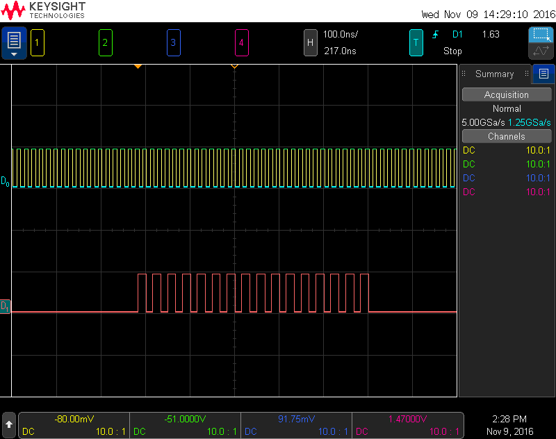
    This shows that the base of the FPGA address space was in R3 to start with and that it then used an LDMIA to to a burst fetch from that space. Below is the 'scope trace :

    D0 is the clock and D1 is the Read strobe signal. You can see it definitely toggles between reads. It toggles 16 times because the data bus is only 16 bits wide and it is trying to do 32 bit fetches, hence 2 cycles per register.

    Best regards,

    Pat.