This thread has been locked.

If you have a related question, please click the "Ask a related question" button in the top right corner. The newly created question will be automatically linked to this question.

Tiva TM4C123 side of SPI interface

Other Parts Discussed in Thread: TM4C123GH6PM, TDC7200EVM

Hi

I am new to the embedded processors world and am trying to get my first SPI interface to work.

I am trying to tackle it by first getting the micro controller side pins to take on their correct values.

In particular I have had no luck getting a clock signal on the CLK out pin. I downloaded a program from

Jonathan Valvano's "starter files" page. See the listing below. While the original file used an external device

(DAC) I have tried to make a generic interface that anyone developing spi code on a TM4C platform might find

helpful - esp when starting out. The code below compiles without errors. I connect an oscilloscope to pin PA2

and get no response. I was of course expecting a square wave timing signal.

The code is fairly low level C  - I can't see exactly which line of code sets up PA2 as the clk signal.

Any tips on getting this working would be most appreciated.

//Cut down version (microcontroller side of SPI - debug) of a program from the site:
// users.ece.utexas.edu/.../
// Original Author J.Valvano
// Original program:  MAX549_4C123.zip  For TM4C123 board


#include <stdint.h>
#include "SysTick.h"
#include <stdio.h>
#include <stdlib.h>
#include "C:/ti/TivaWare_C_Series-2.1.2.111/inc/tm4c123gh6pm.h"

// example pins on the generic spi peripheral (excluded here to debug the MC side.)
// to be tested with an oscilloscope - like the clock signal
// Pin 1 ground
// Pin 2 OUTA
// Pin 3 CS, SSI0Fss connected to PA3
// Pin 4 DIN, SSI0Tx connected to PA5
// Pin 5 SCLK SSI0Clk connected to PA2
// Pin 6 OUTB
// Pin 7 REF (cheap solution connects this to +3.3V)
// Pin 8 +3.3V

#define SSI_CR0_SCR_M           0x0000FF00  // SSI Serial Clock Rate
#define SSI_CR0_SPH             0x00000080  // SSI Serial Clock Phase
#define SSI_CR0_SPO             0x00000040  // SSI Serial Clock Polarity
#define SSI_CR0_FRF_M           0x00000030  // SSI Frame Format Select
#define SSI_CR0_FRF_MOTO        0x00000000  // Freescale SPI Frame Format
#define SSI_CR0_DSS_M           0x0000000F  // SSI Data Size Select
#define SSI_CR0_DSS_16          0x0000000F  // 16-bit data
#define SSI_CR1_MS              0x00000004  // SSI Master/Slave Select
#define SSI_CR1_SSE             0x00000002  // SSI Synchronous Serial Port
#define SSI_SR_RNE              0x00000004  // SSI Receive FIFO Not Empty
#define SSI_SR_TNF              0x00000002  // SSI Transmit FIFO Not Full
                                            // Enable
#define SSI_CPSR_CPSDVSR_M      0x000000FF  // SSI Clock Prescale Divisor


int main(void){
  uint8_t data = 7;
  printf("Setup SPI\n");
// assumes: system clock rate less than 20 MHz

  SYSCTL_RCGCSSI_R |= 0x01;  // activate SSI0
  SYSCTL_RCGCGPIO_R |= 0x01; // activate port A
  while((SYSCTL_PRGPIO_R&0x0001) == 0){};// ready?
  GPIO_PORTA_AFSEL_R |= 0x2C;           // enable alt funct on PA2,3,5
  GPIO_PORTA_DEN_R |= 0x2C;             // enable digital I/O on PA2,3,5
                                        // configure PA2,3,5 as SSI
  GPIO_PORTA_PCTL_R = (GPIO_PORTA_PCTL_R&0xFF0F00FF)+0x00202200;
  GPIO_PORTA_AMSEL_R = 0;               // disable analog functionality on PA
  SSI0_CR1_R &= ~SSI_CR1_SSE;           // disable SSI
  SSI0_CR1_R &= ~SSI_CR1_MS;            // master mode
                                        // clock divider for 8 MHz SSIClk (assumes 16 MHz PIOSC)
  SSI0_CPSR_R = (SSI0_CPSR_R&~SSI_CPSR_CPSDVSR_M)+2;
  SSI0_CR0_R &= ~(SSI_CR0_SCR_M |       // SCR = 0 (8 Mbps data rate)
                  SSI_CR0_SPH |         // SPH = 0
                  SSI_CR0_SPO);         // SPO = 0
                                        // FRF = Freescale format
  SSI0_CR0_R = (SSI0_CR0_R&~SSI_CR0_FRF_M)+SSI_CR0_FRF_MOTO;
                                        // DSS = 16-bit data
  SSI0_CR0_R = (SSI0_CR0_R&~SSI_CR0_DSS_M)+SSI_CR0_DSS_16;
  SSI0_DR_R = data;                     // load 'data' into transmit FIFO
  SSI0_CR1_R |= SSI_CR1_SSE;            // enable SSI


}

cheers, Tim

  • Hello Tim,

    I would then suggest to use the TivaWare API instead of the low level DRM approach. There is an example in TivaWare under examples/peripherals/ssi which gives a basic loopback operation.
  • Hi Amit

    Thanks for pointing out the more friendly code ti_master.c. So it seems to be running ok on the TM4C1294 side of the SPI. I can see bursts of activity on the CLK line with the scope when I send values to the slave side.
    I have the TDC2700EVM to connect up next.
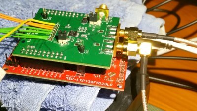
    Can you tell me if I can mount it on the MSP430F to give it power
    and at the same time communicate with it using the SPI connected to the 1294? I would try using the MSP but
    I am reasonably comfortable using the 1294 libraries and includes etc.

    I was thinking I could run the demo code for the 7300 that shows the measured START-STOP times and compare this
    to what I get from the SPI to validate it.

    cheers, Tim
  • Hello Tim,

    I am not sure what you mean by mounting it on MSP430F?
  • Hi Amit

    The TDC7200EVM has 4 rows of 10 pins (in two double banks) and it has been designed to

    connect to the 40 pins on the MSP430F - (it is described here http://www.ti.com/tool/tdc7200evm

    The SPI plus some additional lines to enable the 7200 and interrupt to MCU when data is ready to read

    can be seen soldered on the back of the 7200 and these I connect to the TM4C1294 to save and process

    My question was whether these two connections, one to the 430F and the other as a SPI slave of the

    1294 are going to interfere with each other?

    Tim

  • Hello Tim

    If it is a boosterpack then the same can be mounted on the TM4C129x launchpad/EVM. As long as the SPI signals being used are not being driven by the MSP launchPad it should be OK. However I am not that mounting the boosterpack on the MSP launchpad and using the SPI connections would be non-interfering as I do not the MSP devices power up behavior. You must check that with MSP forum. In either case, I would suggest using the BoosterPack headers on the TM4C launchpad as the better solution.
  • Hi Amit (and anyone else kind enough to follow this thread and offer comments)

    I have been trying to figure out how to read the value of a register on the external device.
    I see that (using the API)
    SSIDataGet(SSI0_BASE, &myvar);

    should put the data in the slave's (TDC720x) output FIFO
    into myvar. But how do I get the register (addr 0x04) into the FIFO?
    Is this a kind of request made using the SSIDataPut command?

    Here is the code. I only get 0s back from the SPI when I should get
    time of flight measures

    cheers Tim
    //
    // This is part of revision 2.1.2.111 of the Tiva Firmware Development Package.
    //
    //*****************************************************************************


    #include "include/TI_TDC720x.h"

    #include <stdint.h>
    #include <stdbool.h>
    #include <stdio.h>
    #include "stdlib.h"
    #include "inc/hw_ints.h"
    #include "inc/hw_memmap.h"
    #include "inc/hw_uart.h"
    #include "inc/hw_gpio.h"
    #include "inc/hw_ssi.h"
    #include "inc/hw_pwm.h"
    #include "inc/hw_types.h"
    #include "driverlib/timer.h"
    #include "driverlib/gpio.h"
    #include "driverlib/interrupt.h"
    #include "driverlib/pin_map.h"
    #include "driverlib/rom.h"
    #include "driverlib/rom_map.h"
    #include "driverlib/sysctl.h"
    #include "driverlib/uart.h"
    #include "driverlib/udma.h"
    #include "driverlib/pwm.h"
    #include "driverlib/ssi.h"
    #include "driverlib/systick.h"
    #include <string.h>


    //! - SSI0Clk - PA2
    //! - SSI0Fss - PA3
    //! - SSI0Rx - PA4
    //! - SSI0Tx - PA5
    //! PA6 INT PA7 ENABLE

    // GLOBALS
    uint32_t NUM_SSI_DATA = 3;
    uint32_t Period, freq, dutyCycle;

    #define START_MEAS 0x00
    #define MODE_MEAS 0x00

    //*****************************************************************************
    void Init_PulseGen() {

    // Port M Pin 1 Port M init in InitPeriod
    SysCtlPeripheralEnable(SYSCTL_PERIPH_GPIOM);
    SysCtlDelay(3);
    GPIOPinConfigure(GPIO_PM1_T2CCP1);
    GPIOPinTypeTimer(GPIO_PORTM_BASE, GPIO_PIN_1);

    printf("Sys Clock = %d \n",SysCtlClockGet());
    Period = SysCtlClockGet()/freq ; //freq defined in main
    dutyCycle = Period/2;
    SysCtlPeripheralEnable(SYSCTL_PERIPH_TIMER2);
    SysCtlDelay(3);
    TimerConfigure(TIMER2_BASE, TIMER_CFG_SPLIT_PAIR|TIMER_CFG_B_PWM);
    TimerLoadSet(TIMER2_BASE, TIMER_B, Period);
    TimerMatchSet(TIMER2_BASE, TIMER_B, dutyCycle); // PWM

    SysCtlDelay(3);
    TimerLoadSet(TIMER2_BASE, TIMER_B, Period);
    TimerMatchSet(TIMER2_BASE, TIMER_B, dutyCycle); // PWM
    //Turn on timer
    TimerEnable(TIMER2_BASE, TIMER_B);

    } // end PWM
    //*****************************************************************************

    int
    main(void)
    {
    uint32_t ui32SysClock;
    uint32_t clockrate = 120000000; //set system clock to run at 32MHz
    uint32_t timeresult, junk;
    uint32_t dummy = 99; // used to drive retrieval if needed

    // Set the clock
    SysCtlMOSCConfigSet(SYSCTL_MOSC_HIGHFREQ);
    ui32SysClock = SysCtlClockFreqSet((SYSCTL_XTAL_25MHZ |
    SYSCTL_OSC_MAIN |
    SYSCTL_USE_PLL |
    SYSCTL_CFG_VCO_480), clockrate);
    SysCtlDelay(3);
    printf("ui32SysClock = %d\n",ui32SysClock);
    // The SSI0 peripheral must be enabled for use.
    freq = 3250;
    Init_PulseGen(); // drives an ultrasonic TxRx : out (START Pin) return (STOP pin) of TDC720x

    //
    // The SSI0 peripheral must be enabled for use.
    SysCtlPeripheralEnable(SYSCTL_PERIPH_SSI0);
    //
    SysCtlPeripheralEnable(SYSCTL_PERIPH_GPIOA);
    SysCtlDelay(3);
    //

    GPIOPinConfigure(GPIO_PA2_SSI0CLK);
    GPIOPinConfigure(GPIO_PA3_SSI0FSS);
    GPIOPinConfigure(GPIO_PA4_SSI0XDAT0);
    GPIOPinConfigure(GPIO_PA5_SSI0XDAT1);

    GPIOPinTypeGPIOOutput(GPIO_PORTA_BASE, GPIO_PIN_3); // slave select (later needs to go to 0)
    GPIOPinTypeGPIOOutput(GPIO_PORTA_BASE, GPIO_PIN_7); // ENABLE Pin set as output

    GPIOPinWrite(GPIO_PORTA_BASE,GPIO_PIN_7, 0); // clear the enable pin for a while at initial start up (per instructions p 20 datasheet)
    SysCtlDelay(10000);
    GPIOPinWrite(GPIO_PORTA_BASE,GPIO_PIN_7, 1); // set the enable pin
    GPIOPinTypeSSI(GPIO_PORTA_BASE, GPIO_PIN_5 | GPIO_PIN_4 | GPIO_PIN_3 |
    GPIO_PIN_2);
    SysCtlDelay(3);
    // Configure and enable the SSI port for TI master mode. Use SSI0, system
    // clock supply, master mode, 1MHz SSI frequency, and 8-bit data.
    //
    SSIDisable(SSI0_BASE);
    SSIConfigSetExpClk(SSI0_BASE, clockrate, SSI_FRF_TI,
    SSI_MODE_MASTER, 1000000, 8); // set SSI clk to run at 1mill bits/sec
    SysCtlDelay(3);
    // Enable the SSI0 module.
    SSIEnable(SSI0_BASE);
    GPIOPinWrite(GPIO_PORTA_BASE,GPIO_PIN_3, 0); // slave select low
    // Read any residual data from the SSI port.
    while(SSIDataGetNonBlocking(SSI0_BASE, &junk))
    {
    }

    SSIDataPut(SSI0_BASE,0x00); // specify the config1 register on the TDC720x (first register on 7200)
    SSIDataPut(SSI0_BASE,0x01); //start bit is set
    // ??????? not sure if this is how one changes the 0 bit in the first register
    while(SSIBusy(SSI0_BASE)); // wait to ensure transmission complete

    while (1) {

    SSIDataPut(SSI0_BASE,0x10); // specify the time1 register on the TDC720x
    SSIDataPut(SSI0_BASE,0x7FFFFF); // bits 0 to 22 contain the time measurement
    //????? this is where Im unsure of how to extract the contents of the TIME1 register

    // polling version where read waits for the FIFO to fill up
    SSIDataGet(SSI0_BASE,&timeresult); // fetch whatever is on the FIFO (always 0)
    printf("RT = %d\n", timeresult);

    GPIOPinWrite(GPIO_PORTA_BASE,GPIO_PIN_6, 0); // reset interrupt
    SSIDataPut(SSI0_BASE,0x00); // specify the config1 register on the TDC720x
    SSIDataPut(SSI0_BASE,0x01); //start bit is set
    while(SSIBusy(SSI0_BASE)); // wait to ensure transmission complete

    }

    }
  • tim cutmore said:
    Is this a kind of request made using the SSIDataPut command?

    Yes, you send bytes out of the SSI port with that command.

    A few things to check:

    - Are you enabling the FSS line? Is it properly configured and tested? Do you see a clock on the CLK line when you put data?

    - Are you sending the correct content according to your device's datasheet?

    - Typically, you send a question/register in one spi transfer, and the device returns the information on the following transfer - at the end, you need to send a dummy byte to read the "last reply".

    - You may want to wait for the spi line to be free (check SSIBusy) between that first and second transfer.

    If the device works on this typical "receive the question in one transfer, answer on the next", then you don't have to poll anything: right after you send the second byte, the response WILL be on your Rx buffer - just read it. If there is nothing valid there, it means your device did not reply properly (either it is not wired correctly, or you did not send the right question).

    Cheers

    Bruno

  • It's my belief that "question" should be replaced w/"Command."

    For eternity such transactions operated under the name, "Command/Response."
    As the devices become more complex - such "commands" may extend into multi-byte or even 16 bit format...
  • Amem to that!
    I did exaggerate simplifying the terms to those of mere mortal domains! Myself again never formally being introduced to these terms did not use the formal Command/Response!
  • Nothing wrong w/your approach. Yet - poster may wish to "read/review" the (history) of such device interchange. "Command-Response" is FAR better represented than "question." (I'd never/ever encountered "question.")
  • I would heartily suggest not using not using FSS. It's only suitable for a subset of cases and questionable for some of those. Use a gpio pin instead, simpler and more robust.

    Robert
  • Hello Tim,

    The TM4C SSI works by putting one DSS size word to get DSS size word. Even when using the Write mode to write to a slave, the SSIDataGet must be called to flush out the data sampled on the MISO line. So first of all every SSIDataPut must have a SSIDataGet.

    The second point is about the data transfer. The SSI Data register is the transmit and receive FIFO entry point. A write to the register puts the data into the transmit FIFO. A read from the register pulls the data from the receive FIFO.