This thread has been locked.

If you have a related question, please click the "Ask a related question" button in the top right corner. The newly created question will be automatically linked to this question.

EK-TM4C123GXL: TM4C123GXL external SPI ADC (Maxim MAX11060)

Part Number: EK-TM4C123GXL
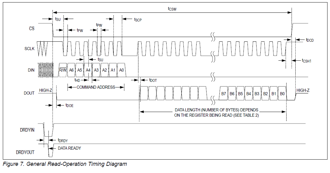
Hey guys I'm having issues reading from my external ADC via SPC and can't seem to find the problem. At the moment I'm just constantly receiving 0s back from the ADC. The ADC I'm using is the MAX11060 (https://datasheets.maximintegrated.com/en/ds/MAX11040K-MAX11060.pdf)  and I'm unsure what is wrong, I've included all my code below. 

Thank you


#include <stdio.h> #include <stdlib.h> #include <stdint.h> #include <stdbool.h> #include <string.h> #include <inttypes.h> #include "inc/hw_memmap.h" #include "inc/hw_types.h" #include "driverlib/adc.h" #include "driverlib/debug.h" #include "driverlib/fpu.h" #include "driverlib/gpio.h" #include "driverlib/pin_map.h" #include "driverlib/rom.h" #include "driverlib/sysctl.h" #include "driverlib/uart.h" #include "utils/uartstdio.h" #include "inc/tm4c123gh6pm.h" #include "inc/hw_i2c.h" #include "inc/hw_gpio.h" #include "driverlib/i2c.h" #include "driverlib/interrupt.h" #include "driverlib/timer.h" #include "inc/hw_pwm.h" #include "driverlib/timer.h" #include "driverlib/interrupt.h" #include "driverlib/rom_map.h" #include "driverlib/udma.h" #include "driverlib/pwm.h" #include "driverlib/ssi.h" #include "driverlib/systick.h" // VARIABLE DECLARTATIONS //================================================================================================================= #define NUM_SSI_DATA 2 uint32_t ui32Loop,ui32Index; uint32_t pui32DataTx[NUM_SSI_DATA]; uint32_t pui32DataRx[NUM_SSI_DATA]; //================================================================================================================= #define UART_BAUD_RATE 115200 void ConfigureUART(void) { /* Enable the GPIO Peripheral used by the UART */ ROM_SysCtlPeripheralEnable(SYSCTL_PERIPH_GPIOA); /* Enable UART0 */ ROM_SysCtlPeripheralEnable(SYSCTL_PERIPH_UART0); /* Configure GPI Pins for UART mode */ ROM_GPIOPinConfigure(GPIO_PA0_U0RX); ROM_GPIOPinConfigure(GPIO_PA1_U0TX); ROM_GPIOPinTypeUART(GPIO_PORTA_BASE, GPIO_PIN_0 | GPIO_PIN_1); /* Use the internal 16MHz oscillator as the UART clock source */ UARTClockSourceSet(UART0_BASE, UART_CLOCK_PIOSC); ROM_UARTConfigSetExpClk(UART0_BASE, ROM_SysCtlClockGet(), UART_BAUD_RATE, (UART_CONFIG_WLEN_8 | UART_CONFIG_PAR_NONE | UART_CONFIG_STOP_ONE)); /* Initialize the UART for console I/O */ UARTStdioConfig(0, UART_BAUD_RATE, 16000000); /* Enable the UART interrupt */ ROM_IntMasterEnable(); ROM_UARTIntClear(UART0_BASE, ROM_UARTIntStatus(UART0_BASE, false)); ROM_UARTIntEnable(UART0_BASE, UART_INT_RX | UART_INT_RT); ROM_IntEnable(INT_UART0); } void SPIWrite(uint32_t Addr,uint32_t Val){ while(SSIDataGetNonBlocking(SSI2_BASE, &pui32DataRx[0])){} pui32DataTx[0]=Addr;pui32DataTx[1]=Val; SSIDataPut(SSI2_BASE, pui32DataTx[0]); SSIDataPut(SSI2_BASE, pui32DataTx[1]); while(SSIBusy(SSI2_BASE)){} } void SPIRead(uint32_t Addr){ while(SSIDataGetNonBlocking(SSI2_BASE, &pui32DataRx[0])){} SSIDataPut(SSI2_BASE, (Addr|0x80)); SSIDataGet(SSI2_BASE, &pui32DataRx[0]); while(SSIBusy(SSI2_BASE)){} UARTprintf("\nData Received: %i ", pui32DataRx[0]); } void main(void){ ROM_FPULazyStackingEnable(); // Set the clocking to run directly from the crystal. SysCtlClockSet(SYSCTL_SYSDIV_8 | SYSCTL_USE_PLL | SYSCTL_XTAL_16MHZ | SYSCTL_OSC_MAIN); ConfigureUART(); // Function for Initializing the UART Protocol SysCtlPeripheralEnable(SYSCTL_PERIPH_SSI2); SysCtlPeripheralEnable(SYSCTL_PERIPH_GPIOB); SSIDisable(SSI2_BASE); SSIClockSourceSet(SSI2_BASE, SSI_CLOCK_SYSTEM); GPIOPinConfigure(GPIO_PB4_SSI2CLK); GPIOPinConfigure(GPIO_PB5_SSI2FSS); GPIOPinConfigure(GPIO_PB6_SSI2RX); GPIOPinConfigure(GPIO_PB7_SSI2TX); GPIOPinTypeSSI(GPIO_PORTB_BASE, GPIO_PIN_7 | GPIO_PIN_6 | GPIO_PIN_4); SSIConfigSetExpClk(SSI2_BASE, SysCtlClockGet(), SSI_FRF_MOTO_MODE_0, SSI_MODE_MASTER, 1000000, 8); GPIOPinTypeGPIOOutput(GPIO_PORTB_BASE, GPIO_PIN_5); GPIOPinWrite(GPIO_PORTB_BASE, GPIO_PIN_5, GPIO_PIN_5); SSIEnable(SSI2_BASE); SSIConfigSetExpClk(SSI2_BASE, SysCtlClockGet(), SSI_FRF_MOTO_MODE_0, SSI_MODE_MASTER, 1000000, 8); SSIEnable(SSI2_BASE); GPIOPinWrite(GPIO_PORTB_BASE, GPIO_PIN_5, 0); SPIWrite(0x60,0x34); //SPIWrite(0x60,0xF0); SPIRead(0xE0); GPIOPinWrite(GPIO_PORTB_BASE, GPIO_PIN_5, GPIO_PIN_5); SSIDisable(SSI2_BASE); UARTprintf("\nEnd of Program..."); }

  • Looking quickly - both your functions "SPIWrite() & SPIRead()" start w/"SSIDataGetNonBlocking()" w/in the top of your "while" loop. Is it not more common to initiate SPI via an SSIPut() - and follow that w/SSIGet()? I've not used this vendor's SPI API in awhile - but believe this to warrant your investigation.

    Your use of a scope clearly will, "speed, ease & enhance" both your - and all others - diagnostic efforts. Nothing can compete w/seeing your SPI Clock and "locked data" march across the screen. Minus that insight - "hope, prayer" rise (close) to your best bet.

    Your SPI device should be emplaced on a proper board - properly inter-connected - and properly powered.      Is that (really) the case?      High performance devices (we assume that's what your's is) - most always - take "not kindly" to breadboards - our hope is that you've invested in an official Eval Board.

    While it is (sometimes) possible to "debug SPI" w/out a scope - the extra time, effort proves draining (and not always successful) - perhaps you can borrow one from a local school or similar.

  • Hi John,

     Some comments and suggestions.

     1. You write SPIRead(0xE0). Inside SPIRead() you OR 0xE0 with 0x80 which still 0xE0. 0xE0 means to read the configuration. Do you meant to read the data register. If this is the case you should be giving SPIRead(0x70).

     2. It seems that as soon as you configure the ADC you immediately try to read the conversion data. Your code has SPIWrite() followed by SPIRead(). There is a latency to which the digital conversion result is available. The signal-delta ADC is normally even slower than the SAR type. I see below from the datasheet.

    The latency of the converter is specified by the following equation: Latency = (5.5 x tDOUT) + (PHI x 1.3μs) + 30μs where tDOUT is the data output period (inverse of the programmed sample rate) determined by XINCLOCK and the selected output data rate, and PHI is the programmed sampling instant delay for the channel in question (0 ≤ PHI ≤ 255). The latency is approximately 374μs at 16ksps.

    3. With the above said, shouldn't you key off of your data read after the DRDYOUT is asserted to the MCU to indicate the data is ready for retrieval?

  • Hi Charles,

    Is it not interesting how you take, "MCU centric" approach - while I vector to: "User's Scope, Eval Board for the ADC, and proper power & interconnect?"

    Minus a scope - and user report/feedback - a "swamp" may await...
  • Looking at the format of the SPI communications for the Maxim chip I think you need data to come out when CS goes low and then clocked on the falling edge of the clock and shifted on the rising edge.

    The TI description for this format is polarity = 1, phase = 0;

    The driver software refers to that as SSI_FRF_MOTO_MODE_2, not mode 0 as you have in your software.

    The other thing I see is that I think you need to add a dummy SSIDataPut() call in your SPIRead() function. To the SPI, every transaction is both a write and a read. The SSIDataPut() function on the master generates the SPI clocks for both a write and a read. The SSIDataGet() function simply returns the value captured by the last SSIDataPut().

  • Bob Crosby said:
    I think you need to add a dummy SSIDataPut() call in your SPIRead() function.

    I thought so too - listed that in my earlier post - and is not a (similar) SSIDataPut() required for his SPIWrite() as well?      (for the identical reason - you've just described.)

    I'd have thought you too would be in Louisville tomorrow - maybe not...

  • Bob,
    You are right about the dummy write to clock out the conversion data.

    I also see below description and this is from the perspective of the ADC. So I think Moto_Mode_0 should be fine.

    A falling edge on SCLK clocks in data at DIN. Data at DOUT changes on the rising edge of SCLK and is valid on the falling edge of SCLK.

    Everything will become obvious if scope is used as suggested by cb1.
  • Charles, CB1,

    I am such a slow poster, both of you answered while I was trying to build my answer checking my formats.

    CB1,

    You are absolutely correct. One picture with a scope can resolve so many SPI format issues. That is what I always do.

    Charles,

    I am not sure format 0 will work. If the Maxim slave does a shift on that first clock rising edge before it clocks in data on the falling edge, both the data read by the slave and that sent to the master will miss the MSb and be left shifted by one. (A scope picture will resolve this.)

    Jordan,

    To be more specific about reading all zeros, you did calls like this:

    SPIWrite(0x60,0x34);

    SSIDataGetNonBlocking() -> should be nothing in the receive FIFO, so nothing done

    SSIDataPut(),  -> write a 0x60, store junk1 (probably 0) in receive FIFO

    SSIDataPut(), -> write a 0x34, store junk2 (probably 0) in receive FIFO

    SPIRead(0xE0);

    SSIDataGetNonBlocking() -> returns junk1 (probably 0, ignored anyway)

    SSIDataPut(); -> write a 0xE0, store junk3 (probabl7 0) in receive FIFO

    SSIDataGet() -> returns junk2 (probably the zero you are seeing)

    So, you need to empty the receive FIFO, do another SSIDataPut() with some dummy data so that the answer from the Maxim is shifted out, and then do another SSIDataGet() to read what was shifted out.

  • Bob,
    You are absolutely correct. Looking at the MAXIM datasheet again, the SPICLK starts high means the clock polarity is 1 not 0, my bad.
  • Hey guys, I think I've made all these changes and I'm now always receiving 128 rather than 0 (after changing polarity). I'll have access to an oscilloscope tomorrow but for now I just wanted to fix any obvious errors in my code. With the SPIRead function I'm not sure I've done this correctly but I have AIN0+ connected to an input voltage, AIN0- connected to ground and all other Analog Inputs (1-4) disconnected completely. The reason I have so much dummy data is because according to the datasheet the data from AIN0 is stored in bits 80-95 of the data register.

    void SPIWrite(uint32_t Addr,uint32_t Val){
    while(SSIDataGetNonBlocking(SSI2_BASE, &pui32DataRx[0])){}
    pui32DataTx[0]=Addr;pui32DataTx[1]=Val;
    SSIDataPut(SSI2_BASE, pui32DataTx[0]);
    SSIDataPut(SSI2_BASE, pui32DataTx[1]);
    while(SSIBusy(SSI2_BASE)){}
    }
    
    void SPIRead(uint32_t Addr){
    while(SSIDataGetNonBlocking(SSI2_BASE, &pui32DataRx[0])){}
    SSIDataPut(SSI2_BASE, (Addr|0x80));
    SSIDataPut(SSI2_BASE, 0);
    SSIDataPut(SSI2_BASE, 0);
    SSIDataPut(SSI2_BASE, 0);
    SSIDataPut(SSI2_BASE, 0);
    SSIDataPut(SSI2_BASE, 0);
    SSIDataPut(SSI2_BASE, 0);
    SSIDataPut(SSI2_BASE, 0);
    SSIDataPut(SSI2_BASE, 0);
    SSIDataPut(SSI2_BASE, 0);
    SSIDataPut(SSI2_BASE, 0);
    SSIDataGet(SSI2_BASE, &pui32DataRx[0]);
    SSIDataPut(SSI2_BASE, 0);
    SSIDataGet(SSI2_BASE, &pui32DataRx[1]);
    while(SSIBusy(SSI2_BASE)){}
    UARTprintf("\nData Received: %i ", pui32DataRx[0]);
    UARTprintf("\nData Received: %i ", pui32DataRx[1]);
    }
    
    
    void main(void){
    
    ROM_FPULazyStackingEnable();
    
    // Set the clocking to run directly from the crystal.
    
    SysCtlClockSet(SYSCTL_SYSDIV_8 | SYSCTL_USE_PLL | SYSCTL_XTAL_16MHZ | SYSCTL_OSC_MAIN);
    
    
    ConfigureUART(); // Function for Initializing the UART Protocol
    
    SysCtlPeripheralEnable(SYSCTL_PERIPH_SSI2);
    SysCtlPeripheralEnable(SYSCTL_PERIPH_GPIOB);
    SSIDisable(SSI2_BASE);
    SSIClockSourceSet(SSI2_BASE, SSI_CLOCK_SYSTEM);
    
    GPIOPinConfigure(GPIO_PB4_SSI2CLK);
    GPIOPinConfigure(GPIO_PB5_SSI2FSS);
    GPIOPinConfigure(GPIO_PB6_SSI2RX);
    GPIOPinConfigure(GPIO_PB7_SSI2TX);
    
    GPIOPinTypeSSI(GPIO_PORTB_BASE, GPIO_PIN_7 | GPIO_PIN_6 | GPIO_PIN_4);
    
    SSIConfigSetExpClk(SSI2_BASE, SysCtlClockGet(), SSI_FRF_MOTO_MODE_2,
            SSI_MODE_MASTER, 1000000, 8);
    
    GPIOPinTypeGPIOOutput(GPIO_PORTB_BASE, GPIO_PIN_5);
    GPIOPinWrite(GPIO_PORTB_BASE, GPIO_PIN_5, GPIO_PIN_5);
    
    SSIEnable(SSI2_BASE);
    
    GPIOPinWrite(GPIO_PORTB_BASE, GPIO_PIN_5, 0);
    
    SPIWrite(0x60,0x34);
    
    //SPIWrite(0x60,0xF0);
    
    SysCtlDelay(4000);
    
    SPIRead(0x70);
    
    GPIOPinWrite(GPIO_PORTB_BASE, GPIO_PIN_5, GPIO_PIN_5);
    
    SSIDisable(SSI2_BASE);
    UARTprintf("\nEnd of Program...");
    
    }

  • Jordon Rolley said:
    I have AIN0+ connected to an input voltage, AIN0- connected to ground and all other Analog Inputs (1-4) disconnected completely.

    The presence of (both) AIN0 (±) suggests a differential voltage is to be applied to your (external) ADC.     That often forces two requirements upon you: 1) either or both of those 2 inputs may NOT extend to the "full rail voltage" of the ADC  (it is the "tie of AIN0 (-) to ground" which concerns) and 2) the ADC's set-up/config code may specify different codings to switch from "single-ended" to "differential."     I believe that today's post presents your first mention of "differential" analog input.

    You advised that all other ADC inputs are disconnected - (thus may "float") - and that is not a universally accepted practice re: ADC inputs.     The ADC spec sheet should be reviewed for proper handling & termination - I suspect that "proper" handling would see each of those ADC inputs - rather than left to "float" -  tied to a safe, "mid-level voltage"  (centered) w/in the ADC's input voltage specification.

    All of those "dummy SPIPuts()" do add risk (while "severely loitering the scope cap w/meaningless data"!)       Should (any) of the other ADC inputs reside (closer) to ADC Data Register bits "0-15" - would it not prove vastly simpler (and safer) for you to introduce your (proper) voltage into (that - bits "0-15") ADC pin - not AIN0?      (as AIN0 resided "high up the data register bit chain - is it not likely that AIN4 - sits at/around the (more desirable) bits 0-15 register space?)      A simple "re-connect" of your (proper) analog input voltage to that "AINx" pin (residing bits 0-15) eliminates the "onslaught" of dummy SPIPuts() - thus proves worthwhile - does it not?

    Silent is your use of an official Eval Board, a custom board, or (God forbid) "bread-board" and your confirmation of adequate power and interconnects between your MCU board and this external device.    In (any) such new,  "board to board" commissioning exercise - "everything" is "always" suspect!      (i.e. suspected of "guilt/fault" until (proven) "innocent/proper")

  • Hi Jordon,

      Some quick comments on top of cb1. 

      1. Are you sure SysCtlDelay(4000) is enough to cover the conversion time? Why wouldn't you use DRDYDOUT to signal the MCU the conversion data is available for read?

      2. You configure SSI for 8-bit transfer. If you need to read out 96bits of data from Maxim, wouldn't you need to create 12 dummy SSIDataPut(). However, you have 10 SSIDataPut() before you do SSIDataGet().

      3. The SSI FIFO is 8-entry deep. So I think you need to do 8 SSIDataPut() before you do SSIDataGet and then continue with 4 more SSIDataPut() and then SSIDataGet(). You can also try 6 SSIDataPut()->SSIDataGet()->6 SSIDataPut()->SSIDataGet(). Key is to make sure your receive FIFO does not overflow.

      4. Yes, please use the scope to verify what is sent out by Maxim. 

      You will be in good hands with cb1 and Bob. I have a plane to catch in a hour. 

  • Hi Charles,

    Poster will be in "good hands" w/cb1 (only) if he has "picked the winner" and made a "large bet." This ground now ceded to Bob - (mint juleps & pastel sundresses - (either or both - (both ideally)) impossible to resist).