This thread has been locked.

If you have a related question, please click the "Ask a related question" button in the top right corner. The newly created question will be automatically linked to this question.

EK-TM4C123GXL: SPI communication with DWM1000

Part Number: EK-TM4C123GXL

hello everyone ,

i have recently started working with dwm1000 modules and i have a question about how the SPI interface on the board works , this is an example of a transaction between the MCU ( tiva c in my case ) and the dwm1000 module

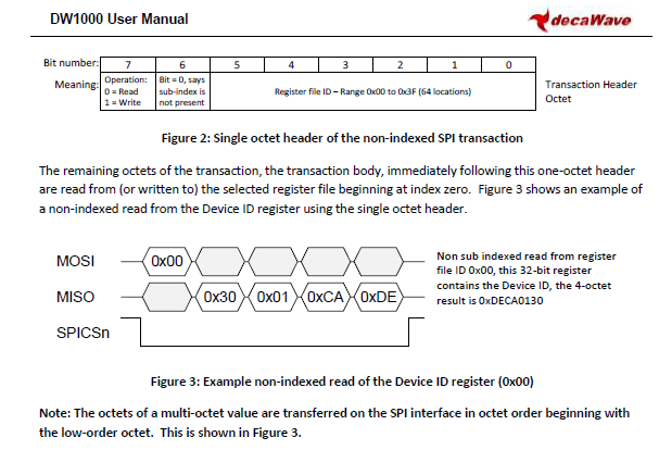
, i am trying to read the register address 0x00 which contains the 0xDECA0130 however since arm microcontrollers work with little endian i should be getting   0x30 0x01 0xCA 0xDE byte order on the bus. 

also note that the SPICS line should be low through the whole transaction , i am using the tivaware api and here is how i initialize and send/read data 

uint8_t DataToSend;
  uint32_t rxDataOne = 0x00;
	uint32_t rxDatatwo = 0x00;
	uint32_t rxDatathree = 0x00;
	// The SSI0 peripheral must be enabled for use.
	SysCtlPeripheralEnable(SYSCTL_PERIPH_SSI2);
	//disable the module first to configure the SPI 
	SSIDisable(SSI2_BASE);
	//enable clock of port b
	SysCtlPeripheralEnable(SYSCTL_PERIPH_GPIOB);
	//Set IO clock as SSI clock source
	//SSIClockSourceSet(SSI2_BASE, SSI_CLOCK_SYSTEM);
	//
	GPIOPinConfigure(GPIO_PB4_SSI2CLK);
	GPIOPinConfigure(GPIO_PB5_SSI2FSS);
	GPIOPinConfigure(GPIO_PB6_SSI2RX);
	GPIOPinConfigure(GPIO_PB7_SSI2TX);
	//
	while(!SysCtlPeripheralReady(SYSCTL_PERIPH_SSI2));
	GPIOPinTypeSSI(GPIO_PORTB_BASE,GPIO_PIN_7|GPIO_PIN_6|GPIO_PIN_5|GPIO_PIN_4);
	SSIConfigSetExpClk(SSI2_BASE, SysCtlClockGet(), SSI_FRF_MOTO_MODE_0,SSI_MODE_MASTER, 2000000, 8);
	SSIEnable(SSI2_BASE);
	//configure data to send here
	DataToSend=0x00;
	//send data
	SSIDataPut(SSI2_BASE,DataToSend);
	while(SSIBusy(SSI2_BASE));
	SSIDataGet(SSI2_BASE,&rxDataOne);
	SSIDataGet(SSI2_BASE,&rxDatatwo);

now i am suspecting this is due to i am using data get and data put to read and write to the bus and the tivaware api is de-aserting  the SPICS between SSIDataPut and SSIDataGet functions , and it should be set to low through the whole transaction however since i am using 2 functions to read and write it turns it back to high after sending the first byte of data for example which would explain why i am only getting 1 byte of data and not anymore from the module . 

if the above is correct i should modify my code to control the SSI CS pin manually through software am i correct ? 

BR,
Essam.

  • i would also like to add that my pin connections for spi mode are the SPIPHA on ground and SPIPOL on ground as well on the DWM1000 board , meaning my mode on the tiva c should be mode 0 as i have done
  • Essam Eid said:
    if the above is correct i should modify my code to control the SSI CS pin manually through software am i correct ? 

    You should do that in any case but you do have another problem.

    Essam Eid said:
    SSIDataPut(SSI2_BASE,DataToSend); while(SSIBusy(SSI2_BASE));

    Here you send one byte

    Essam Eid said:
    SSIDataGet(SSI2_BASE,&rxDataOne); SSIDataGet(SSI2_BASE,&rxDatatwo);

    Here you read that byte back and then do another dummy read. There will not ever be anymore data on an SPI bus regardless of what you do with the chip select.

    On an SPI bus every byte send results in a byte that will be read. And in order to read a byte you must first write one. SPI is just a shift register, every time you clock a bit in a bit is clocked out. And since the first byte you read is just whatever happens to be in the devices shift register when you clock in the command there is a good chance it's meaningless.

    One thing you should get into the habit of doing when first setting up SPI is observing the signal lines on an oscilloscope or logic analyzer. Compare phases and timing to your device requirements. There are multiple possible modes SPI can operate in, only one will be correct, although some incorrect modes may 'almost work'.

    Robert

  • so what you suggest doing is firstly controlling the cs value manually through software that part i understand

    however for the second part , what i understand is when i send data a register number for example using SSIDataPut() then i receive data on the data register fifo and i keep reading byte by byte since the buffer receives all of them , from what i understand is that the SSIDataGet() function moves the data from the data register to a location in the memory i.e. my rxdataone etc. variables.
    thus whats wrong with sending a single "SSIDataPut()" with the register i want to read then using the dataget a couple of times till the fifo is empty ? meaning all the bytes have been read ? since every read operation on the DR of the ssi will remove the current byte read and place the next byte at the top of the buffer ? right ?
  • Essam Eid said:
    however for the second part , what i understand is when i send data a register number for example using SSIDataPut() then i receive data on the data register fifo

    Yes but that data will be whatever happens to be in the devices shift register. It will not be the result of your command since the device cannot have read it yet.

    Essam Eid said:
    i keep reading byte by byte since the buffer receives all of them

    If you do not continue wrinting there is nothing to read. It is the act of writing that produces the clock signal to clock more data.

    In SPI communications each write must have an associated read and likewise each read requires a write.

    Essam Eid said:
    dataget a couple of times till the fifo is empty ? meaning all the bytes have been read ? since every read operation on the DR of the ssi will remove the current byte read and place the next byte at the top of the buffer ? right ?

    Wrong. You must, absolutely must write a byte for each one you read. You must also read a byte for each byte you write. This is fundamental to SPI.

    So if you have a single byte command with a 2 byte response then you would have a sequence something like

    Write command, read dummy

    Write dummy, read response 1

    write dummy, read response 2

    Now the SPI FIFO on these device enables you to write multiple bytes followed by read multiple bytes but you need to make sure you don't overflow the FIFO.  It probably makes more sense for you to start with the simple write a byte, read a byte sequence.

    Robert

  • yea alright i understood your point i didnt know that the clock is not generated when no write operation is used on the MOSI line , so i will try the write command read dummy etc sequence and see if it works ! thanks Robert !
  • @ Robert,

    Great detail - precisely addressing this poster's specifics - could not be more clear.

    The simultaneous arrival of "old" data (unlikely to be useful) "in sequence" w/transmitting (valid) SPI data - is missed by many.

    Your crystal clear example, "Write dummy, read response n" cannot be improved - and should be the "model" for MCU manuals - even those (beyond) this vendor...

    The absence of such clarity - w/in vendor's MCU manual AND code examples - continues to "trip-up" many users - exactly as this post memorializes... (and a "smart vendor" would exploit your "model" - yet it is destined to (shortly) rotate into forum oblivion...)