This thread has been locked.

If you have a related question, please click the "Ask a related question" button in the top right corner. The newly created question will be automatically linked to this question.

Absolute Max Rating for TM4C Devices

Guru 65710 points

Hello Champs


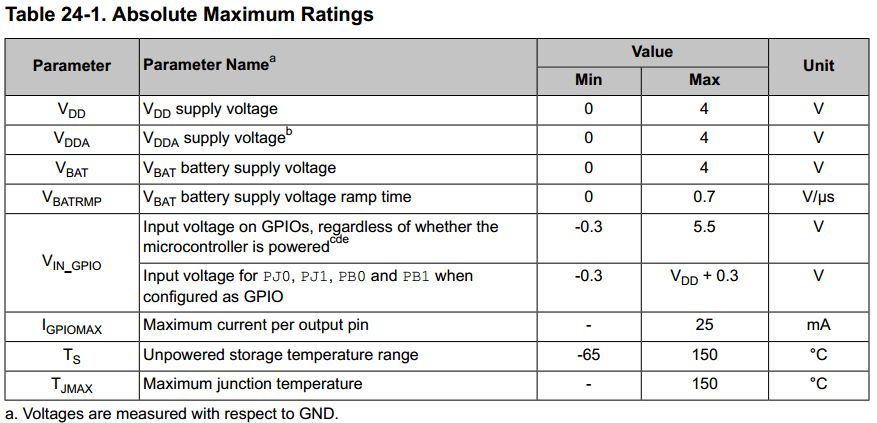
For many TM4C devices, the Data sheet lists 0V as min value.  But it is impossible that the voltage would always stay greater 0V under all circumstances.

I checked many other TI digital ICs, such as MSP430/420, they listed -0.3V instead 0V.


Could you please help me understand why 0V is listed here?


Regards


Yihe

  • To be honest, I do not know. Other devices made using the same process use -0.3V as the absolute minimum on the supply.
  • Several of our large clients have noted such as well. Together - we devised several tests - always keeping in mind that "Absolute Maximum Ratings" are to be avoided - users should strive to remain w/in "normal/customary" operating levels and/or conditions.

    Our tests determined that the "protection devices" (w/in the TM4C MCU series) and the MCU itself - were "well able" to survive (even) long term exposure to voltage levels at/around -0.3V.    (especially so when currents were limited)

    This (-0.3V) voltage level (may) have resulted as being "representative" of (slight) differences in "Ground potential" - often encountered when multiple boards are interconnected - and "common ground" carries sufficient current.     It should be noted that (similar) MCUs - from others - appear to converge to this -0.3 to -0.4V "Abs. Max" (lower) level...

    While NOT recommended - the imposition of series resistors may (even) allow voltages more negative than -0.3V - provided their duration is slight and current is well limited.

    It proves always best to remain w/in "Recommended Operating Conditions" - "Absolute Maximums" should be avoided as they place undue stress upon the device - which may not be immediately detected - and are likely to lead to premature failure...

  • Interestingly enough, whoever wrote the table did mind to tolerate -0.3V on the GPIO pins. The restriction would read only for Vdd, Vdda and Vbat.

    I understand that quick "spikes" of -0.1V on either of those lines can only mean that the MCU is unpowered, and whatever it is, the 3V3 power supply is disabled. When cb1 refers to tests they made in the past, is this the situation you evaluated? Applying a small negative voltage into the power supply pins of an unpowered MCU?

    Bruno

  • Hi Bruno,

    Have to wonder if (Vin_GPIO) is an arbitrary name for MCU external input connections into the PINMUX. To clarify it seems illustrations of peripherals such as ADC and PWM modules rout signals via the PINMUX and seemingly all acquire -0.3v absolute.

    In my opinion for ADC channels that is highly obscure and seemingly holds little weight in light of the evidence ADC (analog) pins can/do operate well below -0.3v without harming MCU silicon.

    It is possible the complete picture of the PINMUX is not being elaborated in the electrical specs to show a unique electrical difference exists between digital and analog PINMUX modes of certain peripherals.