This thread has been locked.

If you have a related question, please click the "Ask a related question" button in the top right corner. The newly created question will be automatically linked to this question.

EK-TM4C123GXL: SSI Configuration

Part Number: EK-TM4C123GXL

Hi,

I am currently trying to set up the SSI module for SPI functionality to grab 8 bits at a time from external flash. I am also running at a desired 66.66MHz clock for a timer function. I have included a snippet of my code below of what I have initialized so far for SSI:

//Enable Peripherals used

ROM_SysCtlPeripheralEnable(SYSCTL_PERIPH_GPIOA);

ROM_SysCtlPeripheralEnable(SYSCTL_PERIPH_GPIOB);

ROM_SysCtlPeripheralEnable(SYSCTL_PERIPH_GPIOC);

ROM_SysCtlPeripheralEnable(SYSCTL_PERIPH_TIMER3);

ROM_SysCtlPeripheralEnable(SYSCTL_PERIPH_SSI2);

///////////////////////////////// Pin Configurations //////////////////////////////////////

//Timer 3A

ROM_GPIOPinConfigure(GPIO_PB2_T3CCP0); //configure function of GPIO Pin (_P#_fucntion)

ROM_GPIOPinTypeTimer(GPIO_PORTB_BASE, GPIO_PIN_2); //configures pin for use by timer

//Audio Amp

ROM_GPIOPinTypeGPIOOutput(GPIO_PORTB_BASE, GPIO_PIN_3); //Using AMP CTL* on board

ROM_GPIOPinWrite(GPIO_PORTB_BASE, GPIO_PIN_3, 0); //Must move resistor to use AMP CTL (PA4)

//SSI

ROM_GPIOPinTypeSSI(GPIO_PORTB_BASE, SSI_CLK | SSI_CS | SSI_RX | SSI_TX); //configures pins for SSI

ROM_GPIOPinConfigure(GPIO_PB4_SSI2CLK);

ROM_GPIOPinConfigure(GPIO_PB5_SSI2FSS);

ROM_GPIOPinConfigure(GPIO_PB6_SSI2RX);

ROM_GPIOPinConfigure(GPIO_PB7_SSI2TX);

//ROM_GPIODirModeSet(GPIO_PORTB_BASE, SSI_CLK, GPIO_DIR_MODE_OUT); //PB4 is output

//ROM_GPIODirModeSet(GPIO_PORTB_BASE, SSI_CS, GPIO_DIR_MODE_OUT); //PB5 is output

//ROM_GPIODirModeSet(GPIO_PORTB_BASE, SSI_TX, GPIO_DIR_MODE_OUT); //PB7 is output (transmit)

//ROM_GPIODirModeSet(GPIO_PORTB_BASE, SSI_RX, GPIO_DIR_MODE_IN); //PB6 is input (receive)

//////////////////////////////////////////////////////////////////////////////////////////


///////////////////////////////// SSI Configuration //////////////////////////////////////

sysClock = ROM_SysCtlClockGet();

SSIConfigSetExpClk(SSI2_BASE, sysClock, SSI_FRF_MOTO_MODE_0, SSI_MODE_MASTER, 333333, 8);

SSIAdvModeSet(SSI2_BASE, SSI_ADV_MODE_READ_WRITE); //mode where data is written/read from the slave

SSIAdvFrameHoldEnable(SSI2); //enables frame hold feature

SSIEnable(SSI2_BASE); //enable SPI module

/////////////////////////////////////////////////////////////////////////////////////////

My main concern is with the "SSIConfigSetExpClk()" function as I feel I do not fully understand its functionality. Particularly the bit rate and clock inputs. 


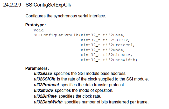
I was hoping I could receive some insight into whether I have missed anything thus far in my initialization of the SSI module. I was also hoping to get some quidance as to how the input clock and bit rate values are determined for this function. Is the sysclock automatically the clock fed into the SSI module? Is there any division of it? How do you determine the bit rate you need?


Thanks,

Garrett

  • The default clock sent to the SSI module is the system clock. It can be programmed to run off of the PIOSC instead. The functionSSIConfigSetExpClk uses the parameters ui32SSICLK and ui32BitRate to determine the pre-scale values to use. Usually the hard thing to configure is the mode. You need to carefully consider the timing diagram requirements of the external flash and compare them to the different timings generated by the TM4C as shown in the datasheet.
  • Hi Bob,

    In considering pre-scale values is there a specific target you try to prescale down to when choosing a timing diagram or are these completely separate?

    Lets take my code for instance. I have the SSICLK = sysClock = 66.66MHz and lets say a bitrate of 333333. I am wanting to sample 8 bits at a time from flash. What doe these inputs mean for me?

    Your help is much appreciated.

    Best,
    Garrett
  • Your system clock is 66.66MHz and the baud rate you requested is 333.333KHz. That means the SPI baud rate is 1/200 of the system clock. That division is taken care of in the SSICR0 and SSICPSR registers. The time to transfer 8 bits is 24uS plus overhead. (8/333333Hz)
  • Thank you for clearing this up.

    The last consideration is that the system clock (66.66MHz) must be at least twice as fast as the SSIClk correct? If this is true then how can sysClock be used as the input for SSIClk?

    Regards,
    Garrett
  • In master mode the clock supplied to the SSI module must be at least twice as fast as the SSI baud rate (Frequency of the SSICLK pin). In your case, it is 200 times faster so this requirement is met.
  • That is what I was expecting but just wanted to double check. In considering the bit rate, can it be an arbitrary value of must it be some kind of multiple of the SSICLK?
  • There are some limitations. The bit rate is:
    BR=SysClk/(CPSDVSR * (1 + SCR))
    where CPSDVSR is an even value from 2-254 programmed in the SSICPSR register, and SCR is a value from 0-255 programmed in the SSICR0 register.
  • Bob Crosby said:
    ... where CPSDVSR is an even value from 2-254 programmed in the SSICPSR register

    Might you clarify that (only) "even values" are accepted?    (meaning that "odd values" (3,5,7...255) prove improper!)     

    I thought that you had "intended" to write "integral values" (rather than even value) - yet It is (now) suspected that a "cascade of clocked flip-flops" (each dividing by two) leads to this "even value" restriction.      Might you confirm - thank you...

  • Yes, the CPSDVSR divisor must be even. Writing a 1 to the least significant bit is ignored. This is required so that the SPICLK pin can be 50% duty cycle.

  • Thank you - appreciated - and such 50% duty cycle has long resulted from (one or more) flip-flops placed w/in the MCU's internal signal path...