This thread has been locked.

If you have a related question, please click the "Ask a related question" button in the top right corner. The newly created question will be automatically linked to this question.

TM4C1294KCPDT: Sequencing of separate VDD and VDDA rails

Part Number: TM4C1294KCPDT

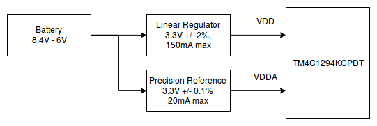
I am designing a system with a TM4C1294KCPDT, which will utilize separate VDD and VDDA rails, as shown below. Please note: I am aware that a buck converter would be a more efficient means to supply VDD, but I prefer the linear regulator because my project is more constrained by cost and complexity than by efficiency. The reason I want a separate VDDA rail is that I want to use the onboard ADCs to make some measurements with precision of 0.25% or better.

The requirements for sequencing VDD and VDDA are not clear to me, as the System Design Guidelines and Datasheet give conflicting requirements:

Datasheet, pg. 1818: "To ensure proper operation, VDDA must be powered up before VDD if sourced from different supplies, or connected to the same supply as VDD. There is not a restriction on order for powering off."

Design Guide, pg 21: "If the VDD and VDDA pins are split, the designer must ensure that VDDA power is applied before or simultaneously with VDD and that VDDA is removed after or simultaneously with VDD."

The datasheet suggests that power-up sequencing will be required in my case, while the design guide says that simultaneous power-up would be acceptable. The two documents also disagree about power-down sequencing. Can someone please clarify for me which document is correct?

Additionally, I would like to know what the quantitative requirements for power-up sequencing are. If I apply the battery voltage to both regulators simultaneously, I may not get simultaneous turn-on at VDD and VDDA due to differences in the current output and the bulk capacitance being driven by each regulator. Both supply rails will rise together, but at different rates. What are the voltage and time relationships that need to be met? The simple qualitative descriptions in the official documentation leave me wondering if a simple soft-start for VDD is sufficient, or if I really need to pick a VDD regulator with an enable input, and force the enable low until the VDDA has 100% completed it's turn-on transient.

  • May I note that (to my mind) you have very nicely "documented & detailed" your issue. Believe such is best handled by vendor staff - who (often) have access to internal documents - withheld from "outsiders."

    Our experience w/MCU ADCs (any ARM vendor) is that - most always - the 3 lsb are "suspect." That said - your target of 0.25% (10 ADC counts) fits w/in those "7 lost counts" registered by such (hopeful) mixed-signal device...

    I would note that over the years - few (i.e. almost none) have made such an in depth, "Prospective Sequencing of Power Rails."      Thus the lack of user posts, "My ADC don't work!" suggests that, "even conflicting vendor guidance" may prove "less than catastrophic!"

  • Hello Oliver,

    The Datasheet is the best reference for situations such as these. I don't know any of the individuals who wrote the System Design Guidelines document, but the datasheet is most reliable on operating condition specifications. I think the Design Guide reference for "or simultaneously with VDD" is more pointing to the idea that when the VDD and VDDA pins are not split, they turn on at once, and thus that is okay with the device. But based on DS specs, the safe thing is to ensure VDDA is being turned on first because when using two supplies, it may not be possible to ensure that VDD doesn't lead VDDA at any point.

    As far as power removal goes, again the datasheet is the better reference. I am not sure where the Design Guide recommendation comes from though it isn't anything outlandish either. I suppose if you really want to have maximum safety you could just apply VDDA first and remove it last, but I really see no reason based on the datasheet that power can't be removed from both at once. After all, the removal of power is not as controllable as sourcing power is!

    As far as a quantitative sequence goes, looking at Table 27-13. Power and Brown-Out Levels, and the sections which discuss the ~POR and POK signals for both VDDA and VDD, I see no dependency that would indicate that VDDA needs to be brought up to full voltage before VDD is brought up at all. To me that makes sense as otherwise I would suspect them being sourced from the same LDO would be problematic. As long as VDDA is leading ahead of VDD consistently, that looks to be fine per the datasheet.
  • Greetings Ralph,

    Great diplomacy - along w/tech insight - upon display.    Just as you noted - (most) semi-firms we've engaged would grant the data-sheet/manual "top dog status!"    Yet - such "notable" conflicts should be "flagged" - for (eventual) study & resolution.    (i.e. right after the "LIKE" is re-instated!)

    Most always VDD encounters a (much) higher (filtering) capacitor load - thus it would rise more slowly (usually) than VDDA.     Yet - when power is removed - those same "caps" will tend to "hold up" VDD - perhaps longer than the more lightly "cap loaded" VDDA.     (note that many linear voltage regulators are sensitive to, "their outputs being higher than their inputs" - which may result when input voltage is suddenly removed - as a result it is not uncommon to find a diode emplaced to "force" VDD to instantly "track" V_Input's removal.)

    As to "Power Turn Off" - this has proved a great issue w/the demanding (multi) supply requirements of both cell & tablet displays.   In many cases - power is (only) religiously/systematically & sequentially "applied & removed" - via the management of multiple supply IC "enables" (just as our poster noted!)      (the main power source (battery) always remains ON - although tasked minimally when the device is "off" - which "allows" such orderly, "Power Switch-On/Off!")

    Again - absent from this forum - is ANY reportage of VDD vs VDDA induced Failures - suggesting that the issue may not be of great consequence...     (especially when compared to the "nightmare" which is "JTAG Lock-Out" - arriving daily - this space...)

  • Ralph,

    Thanks for your reply. Although I am still curious about the discrepancy between the two, I will carry on with my design using the information in the datasheet.
  • Note to anyone who discovers this post and is tempted to use a precision reference for the VDDA supply: I decided not to do this, because I learned that most precision references are not good at driving significant capacitive loads. The VDDA rail would need several microfarads of capacitance, and would draw a few mA.

    The recommended solution for driving a capacitive load from a precision reference is to 'decouple' the output of the reference from the capacitive load with a small resistance. I decided that the voltage drop across this resistance due to VDDA current would be too high, so I have consequently decided to drive VDD and VDDA from the same source, and use my precision reference solely for VREFA+.