


Other Parts Discussed in Thread: TLC555, TPS22969, , TIDA-00195
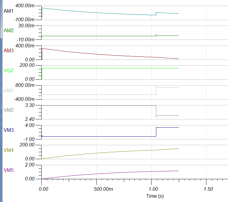
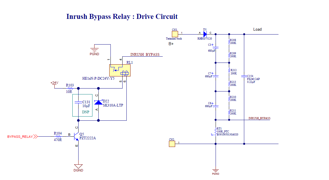
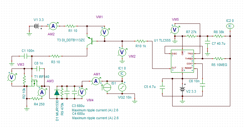
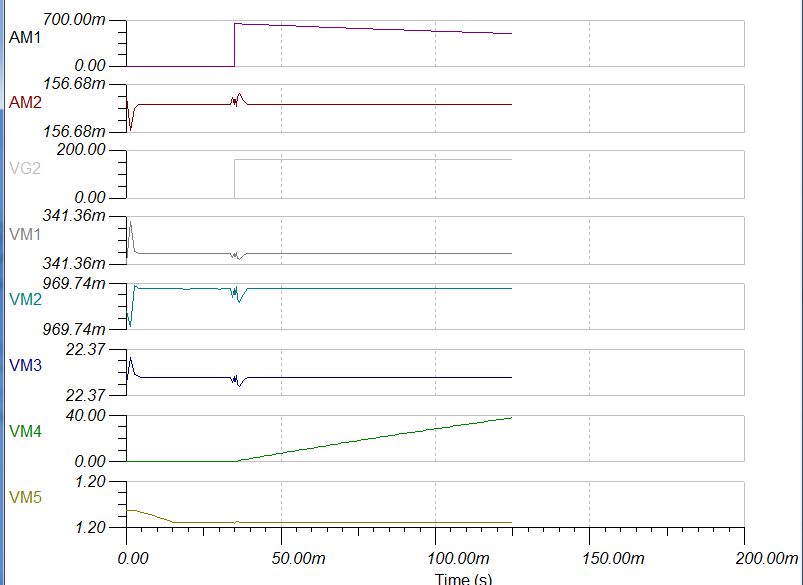
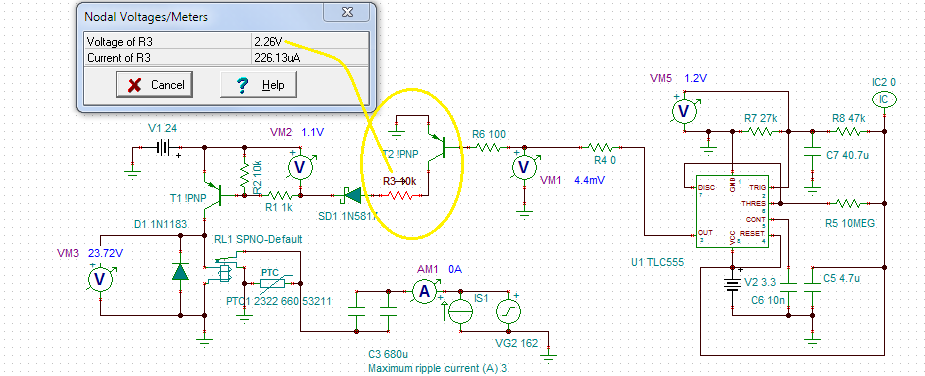
Curious if anyone thinks it dangerous to drive a digital PNP switching 24 volts via GPIO output required to drive a relay? Tina simulations of a similar delay driver circuit seem to suggest that a Schottky diode should reasonably block 21v potential from entering the GPIO pin. Very low current results via R3 yet the potential at cathode SD1 is alarming, does not harm the CMOS TLC555. R1/2 are built into the 500ma PNP digital where E to B must not exceed 5v.
Built a similar circuit 5v relay drive with 1 sec delay for soft starting a 2.5KW toroidal transformer with 13200uf caps to slow down in/out DC rush current.
The digital PNP vendor supplies a Spice text file but I'm not sure where to add those parameters to a user defined block or if that is even possible in the TI version Tina. Wonder if there is a TM4C1294x GPIO port Spice macro or TI library I can import.


