This thread has been locked.

If you have a related question, please click the "Ask a related question" button in the top right corner. The newly created question will be automatically linked to this question.

TM4C123GH6PM: SPI trouble with an MCP23S17 Bus Expander

Part Number: TM4C123GH6PM

I am trying to interface my TM4C123G launchpad with an MCP23S17 Bus Expander.  Presently, I am trying to read a configuration register at address 0x00.  The datasheet on the bus expander states:

The SPI write operation is started by lowering CS. The
Write command (slave address with R/W bit cleared) is
then clocked into the device. The opcode is followed by
an address and at least one data byte.

The SPI Addressing is indicated as 0 1 0 0 ADR2 ADR1 ADR0 R/W A7 A6 A5 A4 A3 A2 A1 A0.  Using HW adsressing 000, so we have a uint32_t that is coded to 0x4100 (Address 0, Read=1) and register address 0x00.  

SSIDataPut(SSI0_BASE, 0x4100);

while (SSIBusy(SSI0_BASE));

SSIDataGet(SSI0_BASE, rxData);

There is 16 clock pulses and the output data is good, but then the clock stops.  Every so often, the input data comes in during the next transmit.  We have been experimenting with trying to send extra bytes to keep the clock active, but we can not get it to work reliably.  I am able to change the address and see the same results with other registers returning the POR default values.  Help please!  Thanks

Looking at the scope, the *CS is good and I see the output SSI0 TX with the 0x4100.  This is immediately followed by a SSIDataGet().  

  • Your code is (very) condensed and does not show the key, "SSIConfigSetExpClk()" function - which has the responsibility of "matching" your MCU's SPI format to that of your SPI Slave. Most always - the MCU enjoys far more "format flexibility" than the Slave - thus it falls upon the MCU to "match" the Slave's format. Does this info meet your understanding - and have you (employed) that function (somewhere) - but withheld it from posting?

    You note 16 clock pulses - and then the clock stops. Does not the clock synchronize to your SPI data output? W hen that data is exhausted it is normal that the SPI clock halts. Is this your understanding - as well?

    Most users here find that (their) control over "SPI_CS" is superior to allowing the MCU to control the "CS." (this is expecially true when 16 bits is selected - at those times the CS signal must precisely comply w/the Slave's timing & signal presentation specs.
  • ROM_SSIConfigSetExpClk(SSI0_BASE, 80000000, SSI_FRF_MOTO_MODE_0, SSI_MODE_MASTER, 1000000, 16);

    I am controlling the *CS as a GPOI and the timing is well within the tolerances specified by the data sheet of the slave device.

    Your explanation of the clock syncing to the data output is how I understand it should operate, but it is not functioning as I expect.  When I write three bytes, I expect to see 24 clock pulses and I do.   However, watching the SI line on the scope (so the input to the MCU, the output from the slave device) I will see the SI line go high most often on the last clock pulse, sometimes the data (0xff) will show up on the next transmit during one of the first two bytes.  I say "show up" meaning that I can validate the data on the scope (SI high for the riding edge of 8 clock pulses). 

  • Thank you - it remains unclear if you've (just added) "ROM_SSIConfigSetExpClk()" - which did not appear w/in your initial posting/code listing.    (I've not time to confirm the parameters you've chosen - insure they are correct - best results usually stem from "slower clocking" during initial "bringing up" of the device)

    We have past (sucessfully) used that exact device - both in its SPI and I2C incarnations.    (we finally chose the I2C version due to the "2 pin" savings..)

    Firm/I are big believers in "KISS" - iirc the simplest task w/that device is "setting & then reading its configuration."    Have you tried that - and if so - what were your results. I recall that we passed (if my recall is correct) only "single byte" commands & data to the device. (as the device was organized into "8 bit ports" - again that's my "years ago" belief.)     Might you try via this, "single byte method" - which simplifies & may "solve" your clocking issue?

    We "test/verified" (both) versions of this "I/O extender" (technically it is "not" an SPI "bus extender") via 16 Leds - one connected to each of the device's I/O.   (a "walking one" (or zero) at reduced speed provides eased device verification...)

    Note that ours worked w/a "carefully implemented bread-board" and our cabling was 8" or less.    Insure that the device voltage (during transactions) is proper & stable & that all connections are secure...

  • It was there all along, just omitted from the original post.
    We are using the I2C version in other projects successfully. The reason I went to the SPI version was to increase the speed of the writes. I'm writing 16 bit outputs to two MCP23017 devices at 4kHz in a closed loop control system. So, between the SPI reads of the ADCs for the control loop feedback, the control loop calculations and then writing the DACs and the bus expanders, which control a digital to synchro converter, I was on the hairy edge of over-running my 250 usec time slice. I implemented some GPIOs and sent them to a scope to evaluate the timing. The 16 bit writes of the DACs using SPI were taking < 10uS (@ 1Mhz bit rate) versus almost 120 uSec for the I2C (high speed 400 kHz) writes to the bus expander. So, to gain some reserve timing, I am trying to replace the I2C bus expanders with SPI bus expanders.
  • You need screen shots I think.

    Brian Savage said:
    When I write three bytes, I expect to see 24 clock pulses and I do.  

    Good.

    Brian Savage said:
    However, watching the SI line on the scope (so the input to the MCU, the output from the slave device) I will see the SI line go high most often on the last clock pulse, sometimes the data (0xff) will show up on the next transmit during one of the first two bytes.  I

    The SI is Slave Input (master output). Full names are MOSI (Master Out Slave In) and MISO (Master In Slave Out).

    If you haven't wired them wrong this sounds like you may have a clock/data phase mismatch. With four different possibilities, that's easy to do.

    Robert

  • You've surely "made the case" for use of SPI - and you are (doubtlessly) skilled & experienced enough to have configured the slave correctly - yet those facts were "not available" w/in your initial post. Many posters "bore us" by reciting vendor's legal "boiler plate" and other "non-issue" code - both of which mask & obscure their "real code issue." Withholding so key a function is not recommended.

    Knowing (now) the significance of your quest - I'll "make the time" today to review the set-up/config. requirements of that SPI device. (may not be until "profit seeking time" expires - i.e. night...)

    As an alternative - have you considered use of a conventional "latch?" Should you have a port w/"uncritical control functions" - you may "share" it w/the latch. (the latched outputs will be stable/secure & are most likely to meet (even exceed) your "speed-up" requirement...)     (note: the latch is "clocked" via a GPIO from a 2nd (different) port - assuming you've employed an 8 bit latch (i.e. HCT373 etc.))

  • Oh, not sure if you are using a logic analyzer or a 'scope. If you are using a logic analyzer, break out an oscilloscope and verify the waveform, make sure that the waveforms are as clean as they should be.

    Robert
  • cb1_mobile said:
    As an alternative - have you considered use of a conventional "latch?"

    I'd normally recommend such over an I/O expander in any case. Less expensive and multiple sourced.

    Robert

  • I'm using an oscilloscope. I've got my wires short and clean and the signals are all nicely shaped and at the proper levels.
  • You have (now) TWO Votes for a "simpler & faster" Latch!
  • It would be wise to post to the I/O extender firm's forum as well - asking what they believe the device's (optimum) throughput to be...   (such "justifies" the expenditure of further time/effort in this behalf)

  • cb1_mobile said:
    an 8 bit latch (i.e. HCT373 etc.))

    A '595 or '165 would make sense (already serial <--> parallel) with appropriate latches. They can use extra control lines though for possible output enable and input latching, although the output enable could be tied to a constant value.

    Robert

  • Indeed - but for the "slowness" of "4C123's" GPIO clocking. (poster is shooting for serious output speed-up)

    Two GPIO writes (one to present data to the latch, second to clock/latch it) trumps the 8 clocks via SIPO.
  • And you could probably get rid of the input latch signal by inverting the CS signal.

    Robert
  • cb1_mobile said:
    Indeed - but for the "slowness" of "4C123's" GPIO clocking. (poster is shooting for serious output speed-up)

    Two GPIO writes (one to present data to the latch, second to clock/latch it) trumps the 8 clocks via SIPO.

    Wouldn't you just put them on SPI? I do.
    Robert
  • If it proves true that, "8 SPI Clocks" occur in a shorter time-frame than "2 GPIO Writes" (via fast bus!) - then the use of such "SIPO & latched" device indeed makes sense. Yet do recall some (here) have (some/slight) belief in KISS - and use of an 8 bit latch meets "KISS" requirement.

    You made a neat observation re: inverting SPI CS - yet there exist '373 and (lesser known) '374 - which iirc - selection from that pair accommodates either CS polarity...   (one may be edge vs. level clocked)

  • I read your SIPO as GPIO, not Serial in parallel out.

    Unless manipulating I/O is slower than SPI then yes the latches will be faster but they do take rather more pins.

    If you need that you may be as far ahead to use a device that brings out the memory bus.

    Robert

  • If memory serves - when I was a "salary man" - the '595 had (yet) to be introduced.    As you well know - the 164 outputs "propagated" in concert w/the shift clock - the added controls (at the cost of pins) made the '595 far more useful.    And - as you note - use of SPI's "clock & data" mates wonderfully.

    Newer/other M4 devices claim SPI clock rates of 50MHz  (M7s reach that too.)     If the '595 accepts that rate - our poster should be "good to go."    (almost)

    Poster has gone (strangely) quiet - have you/I "chased away" another?    (I thought we had a, "Kinder/gentler Robert...")

  • cb1_mobile said:
    Newer/other M4 devices claim SPI clock rates of 50MHz  (M7s reach that too.)     If the '595 accepts that rate - our poster should be "good to go."    (almost)

    I don't think they go that fast, if memory serves they top out at about half that but maybe some of the fast logic ones do better. At 50Mhz, careful layout will be required.

    cb1_mobile said:
    Poster has gone (strangely) quiet - have you/I "chased away" another?    (I thought we had a, "Kinder/gentler Robert...")

    I don't think either of us have been particularly hostile, I think we're just a self-sustaining reaction. No further input required. The OP may just be awaiting a chance to get a word in edgewise.

    Robert

  • It is noted that the (very few) "big city" crickets - "drown out" the "voices of officialdom!"     (likely concocting (another, needless) "LIKE" firing squad...)

  • Chased away? No...fighting fires on other programs I'm involved in working. I'm back at my bench and will be looking at this again for the remainder of the evening. I will keep you posted.
  • Good that - understand Robert & I (share) some "Sense of humor."

    We both have tried to prove of assistance - I (past) did succeed w/that very device - although it was >10 years ago (2006) - and I've zero recollection of the I/O speed we achieved.   (we employed it to control a small, Graphic, Mono Lcd - for that purpose it proved superb...)

  • cb1_mobile said:
    Good that - understand Robert & I (share) some "Sense of humor."

    Is that what we are calling it now?

    Robert

  • Sir - (quiet) - was it not your job to promote (both) ***LIKE*** & "KISS"?
  • Hello Brian,

    Your presentation of the issue is quite detailed, but I feel I am still lacking information to really sink my teeth into from a debug perspective. If you can post more complete code for device and SPI configuration, process of sending data etc. rather than very small snippers, and/or also provide oscilloscope/logic state analyzer shots with the behavior occurring that would be a good next step to help with tracking down the root cause of this issue.
  • waveforms.pdfI work in a closed area, so I am not able to capture the scope images.  I've drawn the scope image when trying to read the register back.  Also, I was able to turn on an output connected to an LED, so it appears I'm writing, I just can't read the registers back, which is not helpful considering it's split with 8 inputs, 8 outputs
     
    Here is the initialization code:

    void SpiInit_SSI0(void) {
    
    	// The SSI0 peripheral must be enabled for use.
    	ROM_SysCtlPeripheralEnable(SYSCTL_PERIPH_SSI0);
    
    	ROM_SysCtlPeripheralEnable(SYSCTL_PERIPH_GPIOA);
    
    	// Configure the pin muxing for SSI0 functions on port A2, A3, A4, and A5.
    	ROM_GPIOPinConfigure(GPIO_PA2_SSI0CLK); // Configure PA2 for the clock
    	// GPIOPinConfigure(GPIO_PA3_SSI0FSS); // Use a GPIO for the *CS function.
    	ROM_GPIOPinConfigure(GPIO_PA4_SSI0RX); // Configure PA4 for the Master Receive
    	ROM_GPIOPinConfigure(GPIO_PA5_SSI0TX); // Configure PA5 for the Master Transmit
    
    
    	// Configure the GPIO settings for the SSI pins. This function also gives
    	// control of these pins to the SSI hardware. Consult the data sheet to
    	// see which functions are allocated per pin.
    	// The pins are assigned as follows:
    	// PA5 - SSI0Tx
    	// PA4 - SSI0Rx
    	// PA3 - SSI0Fss - Not Used - Use as GPIO to control *CS
    	// PA2 - SSI0CLK
    	ROM_GPIOPinTypeSSI(GPIO_PORTA_BASE, GPIO_PIN_5 | GPIO_PIN_4 | GPIO_PIN_2);
    
    	// Configure and enable the SSI port for SPI master mode. Use SSI0,
    	// system clock supply, idle clock level low and active low clock in
    	// freescale SPI mode, master mode, 1MHz SSI frequency, and 8-bit data.
    	// For SPI mode, you can set the polarity of the SSI clock when the SSI
    	// unit is idle. You can also configure what clock edge you want to
    	// capture data on. Please reference the datasheet for more information on
    	// the different SPI modes.
    	ROM_SSIConfigSetExpClk(SSI0_BASE, 80000000, SSI_FRF_MOTO_MODE_0,
    			SSI_MODE_MASTER, 1000000, 8);
    
    	// Enable the SSI0 module.
    	ROM_SSIEnable(SSI0_BASE);
    
    
    	uint32_t pui32DataRx[2];
    
    	// Read any residual data from the SSI port. This makes sure the receive
    	// FIFOs are empty, so we don't read any unwanted junk. This is done here
    	// because the SPI SSI mode is full-duplex, which allows you to send and
    	// receive at the same time. The SSIDataGetNonBlocking function returns
    	// "true" when data was returned, and "false" when no data was returned.
    	// The "non-blocking" function checks if there is any data in the receive
    	// FIFO and does not "hang" if there isn't.
    	while(ROM_SSIDataGetNonBlocking(SSI0_BASE, &pui32DataRx[0])){ }
    
    }

    ========================================================

    I have this test code that performs the read/writes, in the main().

    	SpiInit_SSI0();
    	
    	// Insert Test Code Here
    	
    	GPIO_PORTA_DATA_R |= GPIO_PIN_3; // Toggle the *CS line
    	SysCtlDelay(10);
    	GPIO_PORTA_DATA_R &= ~GPIO_PIN_3;
    	SysCtlDelay(10);
    	GPIO_PORTA_DATA_R |= GPIO_PIN_3;
    	SysCtlDelay(100);
    	
    	uint32_t dataIn[4] = {0xA5};
    	
    	GPIO_PORTA_DATA_R &= ~GPIO_PIN_3; // Pull PA3 (*CS) low
    	SysCtlDelay(50);
    	SSIDataPut(SSI0_BASE,0x40);
    	// while(!SSIBusy(SSI0_BASE));
    	SSIDataPut(SSI0_BASE,0x0A);
    	// while(!SSIBusy(SSI0_BASE));
    	SSIDataPut(SSI0_BASE,0x20);
    	while(!SSIBusy(SSI0_BASE));
    	
    	SysCtlDelay(650); // Hold the *CS line low for some time to allow the data to be clocked out.
    	GPIO_PORTA_DATA_R |= GPIO_PIN_3; // PA3 back to high
    	
    	SysCtlDelay(g_ui32SysClock);
    
    while (1) {
    
    	GPIO_PORTA_DATA_R &= ~GPIO_PIN_3; // Pull PA3 (*CS) low
    	SysCtlDelay(60);
    	SSIDataPut(SSI0_BASE,0x41);
    	// while(!SSIBusy(SSI0_BASE));
    	SSIDataPut(SSI0_BASE,0x0A);
    	// while(!SSIBusy(SSI0_BASE));
    	SSIDataPut(SSI0_BASE,0x00);
    	while(!SSIBusy(SSI0_BASE));
    	SSIDataGet(SSI0_BASE, &dataIn[0]);
    
    
    	SysCtlDelay(650);
    	GPIO_PORTA_DATA_R |= GPIO_PIN_3; // PA3 back to high
    	printf("Data Read from SPI %x %x %x %x\n\n", dataIn[0], dataIn[1], dataIn[2], dataIn[3]);
    	SysCtlDelay(g_ui32SysClock);
    
    
    }
    
    // End of Test Code
  • Do note - earlier post (13 Sept, 06:03) reported a different "SSIConfigSetExpClk()" in answer to my request.   Here is the (past) code:

    Brian Savage said:
                          ROM_SSIConfigSetExpClk(SSI0_BASE, 80000000, SSI_FRF_MOTO_MODE_0, SSI_MODE_MASTER, 1000000, 16);

    and here is the "latest":      ROM_SSIConfigSetExpClk(SSI0_BASE, 80000000, SSI_FRF_MOTO_MODE_0, SSI_MODE_MASTER, 1000000, 8);

    I suggested the change to "8 bits" to (better) comply w/"KISS."    (as both this vendor's MCU and the SPI I/O extender - are 8 bit based.)

    Perhaps this "change" is in response to my direction...    It is unclear if the poster has had adequate time to evaluate the impact of this code change...

  • How about that...I DO read your posts!
  • Indeed - "YOU" are (the) ONE!            (good that)  (PS151 teachers - forcing the young/loud cb1 to classroom's rear would be pleased.)     (maybe)

    Have you had time to "try" under this new code regime?    (somewhere - lurking in our off-site warehouse - sits the "working code" for a simple LMI MCU (28 pin) and your exact Slave device...)

  • I have been working with it for the past several hours with no progress. Same behavior
  • Ouch - feel your pain! Is it correct to note that you can "write to one of the slave's 8 bit ports" - yet not "receive from the other?"

    And that the write "speeds" are too slow for your comfort?

  • I was able to earlier. I have an FET connected with an LED and was able to turn the LED on and off, but that seems to have stopped working. Time to call it a day and look at it again fresh in the morning. Thanks for your help
  • This still sounds to me like a polarity issue. I've more than one configured the wrong polarity and still have had it mostly work. Sometimes I've even had it work correctly and only notice it on a detailed review of the timing where all the margin was gone on the edge in question.

    I'm not familiar with your chip and I don't download files from e2e so I can't comment further on the details you've presented.

    Robert
  • It is intriguing that "polarity violation" can (almost) succeed as you note.     I'd not have expected that.

    Now while you "mock" both cb1 and crack crüe - they noted:

    Had *** LIKE *** not suffered aimless/unwarranted "beheading" - you'd have LONG SINCE reached your (most proper) GURU Status.    (on this - your 2nd "channel" ... I too have a "becalmed/lesser 2nd channel)

    You assist so many (especially this reporter) so great thanks is in order!   (I'd clap more loudly but for my (still) "healing" broken wrist ... and my (proper) fear of "over stimulating" known, problematic PB0/PB1!)

    Congrats - very well earned/deserved!

  • cb1_mobile said:
    It is intriguing that "polarity violation" can (almost) succeed as you note.

    It boils down to operating in a region where the behaviour is undefined (which is not the same as random). When you get the polarity wrong the reader is attempting to clock data in on the same edge that it is changed.

    Since data out will trail the clock edge slightly the reader may have enough time to clock in the previous data, or it might clock in the next data or it might even be inconsistent. For any particular set of parts it might work consistently for year just sitting on the edge of failure.

    As you say not an intuitive result.

    cb1_mobile said:
      (I'd clap more loudly but for my (still) "healing" broken wrist ... Congrats

    Thanks,

    Robert

  • Robert Adsett said:
    it boils down to operating in a region where the behaviour is undefined ... Since data out will trail the clock edge slightly the reader may have enough time to clock in the previous data

    Superbly explained - crack staff (now, properly) "Quaking in their (overly priced) boots!"    (crack vendor may have to supply you w/"Beyond the usual allotment of: "low thread count T Shirts and (leaky) mugs"...it is assumed that you HAVE read the latest "errata" on both "rewards")

    Now - as you (somewhat) defamed, "crack cb1 staff" - they present the following "custom board" - in the assistance of this poster AND a "brand new (pending) requirement for our firm."

    Not too shabby for a "few hours effort!"    As always - board is KISS compliant - note 16 Leds - organized by Port - just as this poster's chip specifies.    For low data rates & "human recognizable" updates - these Leds prove more stimulating and data inclusive (they readily reveal the state of ALL 16 chip pins!) than (even) the best scope.   (or logic analyzer)    And of course our firm maintains many such "efficiency aiding - KISS implementations - so helpful to design/development...    (and making SO HARD to justify vendor's reluctance to embrace, "KISS!"     (which you/I will DO FOR THEM!)

    Note that staff inserted an R-C network to "auto-generate" the chip's Reset.    In addition - chip spec directs "extra action required" when operating under SPI format 1-1.   (did our poster note that?)

    As/if time allows we'll "edit down" the jpg's size - wanted staff to, "See their efforts "On Line."    This SO deserves the restatement of BANNED  *** LIKE ***.

  • @Brian,

    As you may note - both Robert & I have made sustained (serious) efforts in your behalf.      I'm flying shortly - yet printed the essence of the slave's data-sheets - and have our new (home-made) eval board & LPad - for use later in the day or this evening.

    Might you summarize the latest issues?    I recall:

    • inability to "read" from either Slave I/O Port
    • slowed, back to back writes to your (only) Output Port.   (which must mean you have (also) just one input port)
    • latest report seemed to indicate that (at that time) the ability to "write to the output port" also had lessened (possibly disappeared)

    Is this close to factual/current?    (those unfeeling - challenge my memory - (most unkind) - please do update/advise...)

    Earlier I advised that (my recall) was that we past employed (KISS approved) 8 bit ONLY transfers to this (exact) device.    That said - page 16, Figure 3-7 (MCP data-sheet) reveals, "CS low during an entire 16 bit transfer (Device Opcode + Register Address) generated by the MCU.    This (seems) to disqualify the 8 bit (only) transfer mechanism - do you agree?    (or have your tried - and succeeded - via 8 bits only?)   

    It was 2006 (I recall the client who engaged us for this device - thus that date is certain) when I last visited this device - looking @ the "summary of registers" again (i.e. now) I have NO/ZERO retention of what/why we chose & did.    (that code is warehoused - unavailable to me for the next few days)   

    So that we are "on the same page(s)" I'm travelling w/Pgs: 8.9,12,13 & 15-18.   Kindly confirm or note any (pertinent) page you believe has been missed - thank you...

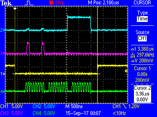
  • I was able to move the test setup out of the closed area and save some scope data.  Above is a "good" read.  Writing 0x4100, Opcode x41, Address x00 which is the GPIO A Direction register.  POR value is 0xFF.

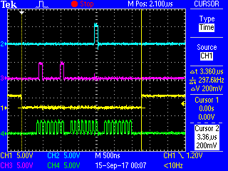
    Unfortunately, this is only the case for about 1 of 5 reads.  I'm reading at 1Hz rate.  The remainder look like this..

    The write of the opcode and the register address are the same, but the response is not.

  • Got it - we (may) have the same 4 channel, mixed signal, Tek scope...

    Was my summary of your issues (near) to correct? (beyond the read trace - presented herein.) Thanks.
    Does your MCP board approximate that which staff made for me?
  • cb1_mobile said:
    That said - page 16, Figure 3-7 (MCP data-sheet) reveals, "CS low during an entire 16 bit transfer (Device Opcode + Register Address) generated by the MCU.    This (seems) to disqualify the 8 bit (only) transfer mechanism - do you agree?

    You just need to keep the chip select valid during multiple transfers, that should only present an issue (maybe) if using the processors chip select mechanism rather than toggling a pin.

    Robert

  • I note that the failed cap reveals (Ch2 blue - Slave Output) as both "premature" and "in error!" You have properly triggered upon CS (Ch1 yellow) driving low (Ch4 green - MCU clock) is equally positioned (each cap) and (as you state) your MOSI data is perfectly consistent!

    So - what then could cause this? Did you note the earlier mention I made of the "Note 1, Fig 1-5, Pg8 MCP manual?" That speaks to the "extra toggling of CS - prior to the first commo after power up. Could that (alone) be your issue?

    As a (sometimes/slight) "disciple of KISS" - do cut your SPI clock rate in half - and re-test. (do humor me - clients so often resist - slow & simple MOST ALWAYS - pays off!)

    Note too that these caps - by themselves - do not provide the ENTIRE MCP picture. The device must have that port (earlier) commanded into Receive Mode - is that not true? Perhaps you've done that - yet that fact is not (yet) in evidence!

    Devil ALWAYS in such details (why some here earn "big bucks") - we WILL resolve this - but I must fly now. (back to you late in the day...)
  • Can you zoom in on the clock/data of the first byte out? The detail's not sufficient to determine the the clocking.

    Robert
  • That is the reason that I chose to use a GPIO to control the CS. If you note in the scope, the clock has a 1 clock cycle delay between each byte. I'm writing three consecutive bytes while holding the CS low.

    I am not able to write the output of the device again.
  • Geez Robert - staff called (me) blind! (is Canadian health/eye care - as bad as our "unaffordable/care-less" mirage?)
  • cb1_mobile said:
    Geez Robert - staff called (me) blind! (is Canadian health/eye care - as bad as our "unaffordable/care-less" mirage?)

    Nah, that's genetics.

    Blowing up to full screen doesn't help though. I think that even with a cursor stepping sample to sample it might be difficult to see what the edges were doing, the entire clock cycle only looks as if it's 1/2 dozen to dozen samples wide. It's a good overview of the transaction though. The good news is that the clocks don't appear malformed.

    Like your idea of slowing it down an order of magnitude or so.

    Robert

  • Robert - while our "Sailing Visit" was delayed (till warmer No. Atlantic waters return) I am prepared to offer you a week's (free usage) of our firm's "Watchdog/Seeing Eye" (bit senior) German Shepherd Rex! He (only) occasionally walks into walls/trees - yet he (surely) can recognize the moon as "more than" a "blob."

    And we're told that there's a "secret" booster pack in development - and should "Plague-Istors R9/R10" be removed - the earth's moon (may) register as (bit beyond) a blob.    (it indeed has been boosted...pay no attention to distortion ... Oh and you may wish to avoid "errata stamped" PB0/PB1!)

  • @Brian,

    I'd prefer we "hold off" on the MCP reads for the time being. (some of our past usage is (slowly) returning to me)

    Please advise your results when employing ideally (both) 8 bit & 16 bit writes to that port designated as Output. Again - do reduce the MCU's SPI clock rate - so that we enjoy the best odds of success.

    If you succeed w/fully controlled writes - then gradually/incrementally increase the clock speed - and present your code which reveals "back to back writes" - which earlier you described as "too slow" to be effective for your Application.
  • Hello Brian,

    Looking at your scope capture, I am in agreement with cb1's observation about how the Ch2 blue - MISO line seems to be going high prematurely. That is the only notable deviance between captures but certainly a significant one. I also endorse his recommended test of slowing the SPI clock rate for the moment so we can observe the result and see if any change occurs.

    Fully understand the slower clock speed may go against final requirements, but first lets see if that helps trace down root cause of the issue being observed.

    Reviewing your code in detail I have a question and then a couple general comments/advice:

    1. Inside your while(1) loop which I assume is what you seeking to show us here, you have 3 DataPut commands, in order: 0x41, 0x0A, 0x00. But the Scope Capture only shows 0x41, 0x00. Did you remove the 0x0A from the process? Curious as the code doesn't match the capture...
    2. You should use MAP commands and not ROM commands. The MAP commands are updated as we update DriverLib to reflect the functions which have been updated since the ROM API's were done so that all API's are using the 'latest and greatest' i.e. 'bug-fixed' API's.
    3. Rather than direct register manipulations for CS, using DriverLib is recommended in general. Rule of thumb overall, though as your CS signal looks fine I see no issue with keeping that as is for now.

    Also, I edited your code post slightly to use the Syntax Highlighter for easier reading. In the future you can make posts like that by using Rich Formatting and then selecting the Syntax Highlighter from the toolbar by looking for the logo with < / >.

  • Ralph Jacobi said:
    Looking at your scope capture, I am in agreement with cb1's observation about how the Ch2 blue - MISO line seems to be going high prematurely.

    Um, I do believe that's a description of the problem, not a diagnosis of its source. The consequence rather than the cause.

    Robert

  • May it be noted that neither vendor's Ralph - nor I - attributed (any) cause/effect to the, "premature onset" of that MISO signal. Such was reported as an "observation" - and due to its (seeming rarity) - quite possibly - worthy of further analysis...

    I did note that "all" MCU SPI clocks seemed consistent - yet a faster "time-base" setting (so that we may visually "catch an SPI clock glitch" (the likely source of that premature MISO emittance) seems, "much in order."

    Noted too is several of my "test requests" have not (yet) received response - I hesitate to add/work more - in their absence...