This thread has been locked.

If you have a related question, please click the "Ask a related question" button in the top right corner. The newly created question will be automatically linked to this question.

TM4C1294NCPDT: Using CAN tx & RX on GPIO pin PB0 & PB1

Part Number: TM4C1294NCPDT

My customer has a major concern regarding the TM4C129.


There were previous issues with the CAN operation, which we concluded  was due to PCB contamination during PCB assembly. We have not seen this failure on a sample of the cleaner PCBs.

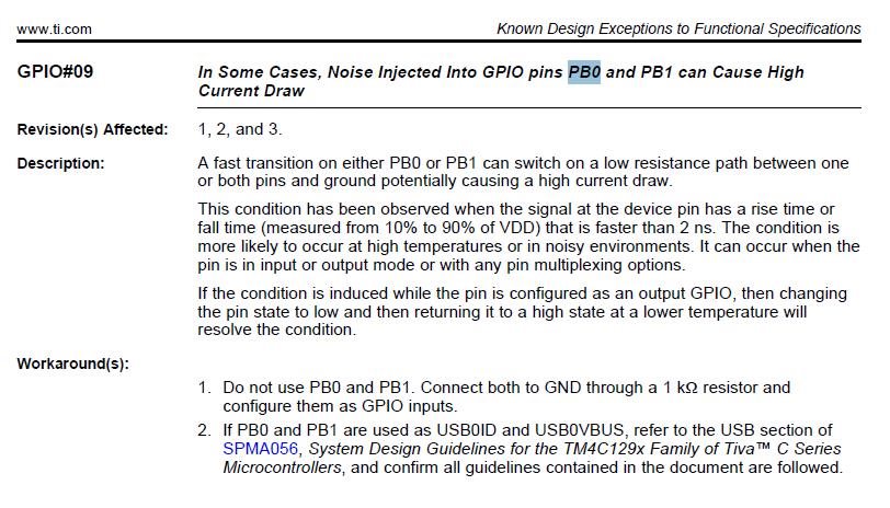
However, reading through the TI errata for the uP and found the following;


Our design has the CAN RX and TX on PB0 & PB1


we are now concerned

1/ that the PCBA cleanliness issue masked an underlying problem which could occur again in the future?

2/ The Ti solution implies that the fix is to not use the PB0 or PB1 pins, unless they are for USB and follow the design guides.


Would you be able to comment if PB0 or PB1 can be used for CAN? The errata implies it cannot if the rise times are fast. please help clarify???

  • nS is GHz signal region. CAN is at most MHz. You should be able to filter the input and output I would think. There was a similar Errata on the '123 that included a filter work-around.

    Maybe the system design guidelines referenced includes such a filter?

    Robert
  • In light of that listed errata - "customer concern" appears highly valid! Use of PB0/PB1 may be like, "Playing w/fire!"

    Other CAN capable pins would seem a "far more suitable choice." (if none are available they'd have to reconfigure (from their initial pin selection) or choose a device w/increased number of pins...)

    Risk/reward must enter such calculation - forcing a "high risk" direction may not prove in your best "long-term" interest...
  • Hello Linda,

    As Robert mentioned, CAN bus signals won't reach a range where that errata would come into play when operating under normal conditions. To prevent any issues with noise or other possible signals, using an RC filter to keep the slew rate above 2ns would be a safe design choice.
  • If this were my design I'd - at minimum - investigate the use of (other) MCU pins - which avoid this "known" sensitivity.
    Casting "risk-reward" to the curb is an "unwise" strategy - may "in time" wreak its havoc - and is (rarely) recommended...

    Having past worked at a similar semi-giant - this weakness may "not" have been fully characterized across: device aging, temperature, voltage and future lot production...

    Sailing directly "into the wind" does NOT work.   (even when adding more sails)     Choosing such hyper sensitive pins should be a (very) last resource - it is likely that (other) CAN capable pins may be employed...

  • Well, that sensitivity is present whether or not you connect the CAN. The only question is how to work around it.

    The same sensitivity is present on all pins of the '123.

    Robert
  • Robert Adsett said:
    The same sensitivity is present on all pins of the '123.

    Must ask - those (same sensitivity - on ALL pins) is not (yet) in evidence.    The errata (very) specifically targets PB0 & PB1!   (by my (repeated) read.)     What leads you to believe that "all pins" SHARE such vulnerability?

    My recommendation would be to "Avoid use of those 2 pins - and terminate them as the errata directs."     Again - that IS in compliance w/the errata's "work-around."

    Best practice would NOT EMPLOY suspect pins!     Pity that a pcb was (earlier) created - yet what potential damage lurks if "issues occur" (at all attributable) to the use of (potentially) problematic pins?   (which was known, "Published, Public Knowledge?"

    Risk-Reward is NOT to be "toyed with!"     (and for what?)

  • cb1_mobile said:
    Robert Adsett
    The same sensitivity is present on all pins of the '123.

    From the '123 Errata April 2016 said:

    GPIO#10 In Some Cases, Noise Injected Into GPIO Pins can Cause High Current Draw

    Revision(s) Affected: 6 and 7.

    Description: A fast transition on any GPIO pin can switch on a low resistance path between the GPIO

    pin or the adjacent GPIO pins and ground potentially causing a high current draw.

    This condition has been observed when the signal at the device pin has a slew rate such

    that the rise time or fall time (measured from 10% to 90% of VDD) is faster than 2ns.

    The condition is more likely to occur at high temperatures or in noisy environments. It

    can occur when the pin is in input or output mode or with any pin multiplexing options.

    If the condition is induced while the pin is configured as an output GPIO, then changing

    the pin state to low and then returning it to a high state at a lower temperature will

    resolve the condition.

    Workaround(s): Limit the slew rate on the IO so that the fastest rise and fall time is greater than 2 ns.

    Use an RC filter or series ferrite to limit the rise and fall times at the device pin. The filter

    capacitor should be placed as close as possible to the device.

    Looks like the same Errata. We ended up applying a handful of resistors and caps to prevent the possibility of exceeding the rate of change limits.


    Robert

  • Thank you - as usual - you ARE able to justify your opinion!      That's very much the "mark of a PRO" - posters should take good note & strive to be able to "justify" their positions.    (i.e. beyond, "I wanna")

    Is it not (very) strange that the errata you've just identified "GPIO 10" (immediately) followed "GPIO 09" - which focused entirely/uniquely upon PB0 & PB1 - yet GPIO 10 patently "avoided" that mention?     Does this not register as "something/somewhere" (possibly) "outside of full control?"

    Firm/I (only) use "123" from this vendor - and "never" have encountered such "excess current draw issues" (we monitor such) yet we have "limited" the use of PB0 & PB1...

  • cb1_mobile said:
    Is it not (very) strange that the errata you've just identified "GPIO 10" (immediately) followed "GPIO 09" - which focused entirely/uniquely upon PB0 & PB1 - yet GPIO 10 patently "avoided" that mention?  

    Not really, they are errata from different chips.

    I mentioned it since it appeared to have shown up in an earlier ICs and had a better detailed fix in the errata for the earlier ICs. The odd part is that the filter wasn't mentioned in the '129 Errata. Also I had implemented the fix on our boards.

    cb1_mobile said:
    Firm/I (only) use "123" from this vendor - and "never" have encountered such "excess current draw issues"

    Your crack team might want to verify that you avoid this problematic condition on the '123. It does affect all the pins on that part. The good news is that on driven pins the drive from the input ICs may be sufficient to prevent an issue. Need to verify against specs though. It also appears to quite rare in application use, I've not run into it either at least that I know of.

    Robert

    If you can find it, somewhere on here, I think Amit and I had a discussion on the issue.

  • As the "crack team" delights in mentioning - there "are" days when I cannot recall my LSD (hi-way) exit... (over-shoot the office by good 5 miles)

    We have far more experience & use w/(past) LX4F device (claimed to be (almost) the same) and have "moved on" to far faster M4s & M7s - not yet "in residence" here...