This thread has been locked.

If you have a related question, please click the "Ask a related question" button in the top right corner. The newly created question will be automatically linked to this question.

TM4C129ENCPDT: Customer is seeing far more jitter than expected

Part Number: TM4C129ENCPDT

Team,

I have a customer that has come to me with the following issue:

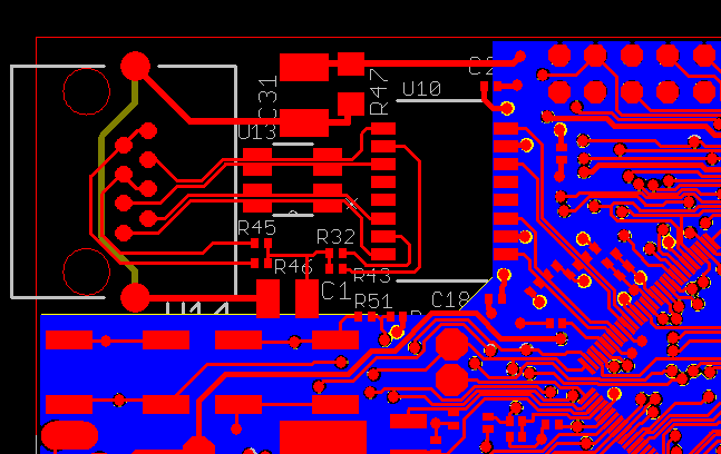
"We have the Tiva™ TM4C129ENCPDT Microcontroller on several of our products. We just purchased an Ethernet test set, Sifos PVA 3002.


We ran 3 of our Tiva boards and see errors in the jitter and noise testing on all 3. I've run my laptop and a router and do not see this as a common or set up error.

The 3 boards are 3 different layouts, but essentially the same design. I've done some experimenting with grounding, clocking, etc, and am unable to enact any improvement. Is this normal for Tiva using internal PHY? The SW guy says he's using the Tiva source code from a few months ago. Nothing outdated. I do not see any mention in errata."

Could you comment on potential reasons for this? They have also sent me schematics and a read-out of their report, but I do not wish to share those here. If needed, could a member of the team contact me off-line.

  • Hello Carolus,

    Have they run similar tests with TI hardware for a comparison point between our reference designs and their own custom boards? Before anything else, I would like them to run these Ethernet tests on our LaunchPad and see what the results are for a baseline to compare our known good reference design versus their own custom boards with.

    Have they been following the System Design Guidelines for schematic/layout?: http://www.ti.com/lit/an/spma056/spma056.pdf - Section 4.1 covers the Ethernet Internal PHY in great detail, have they read through and followed all of these steps?

    What is the MOSC they are using?

    Are they using high quality Ethernet cables for these tests?

  • Dear Ralph,

    Please find responses inline below:

    - Have they run similar tests with TI hardware for a comparison point between our reference designs and their own custom boards? Before anything else, I would like them to run these Ethernet tests on our LaunchPad and see what the results are for a baseline to compare our known good reference design versus their own custom boards with.

    I was just handed the reference board. I'll look on the web page for the software/driver. Your layout is a lot tighter than ours. I'll try and run it tomorrow.

    - Have they been following the System Design Guidelines for schematic/layout?: http://www.ti.com/lit/an/spma056/spma056.pdf - Section 4.1 covers the Ethernet Internal PHY in great detail, have they read through and followed all of these steps?

    I have read these in great detail. We do have some layout violations.

    What is the MOSC they are using?

    I assume you mean oscillator/crystal?

    CRYSTAL, SMD, 25MHZ FUNDAMENTAL, 5MM X 3.2MM, 8pF LOAD CAPACITANCE, 20PPM TOLERANCE.

    Are they using high quality Ethernet cables for these tests?”

    Yes, this is a calibrated cable that comes with the test equipment.

  • Hello Carolus,

    Thank you. Please keep me posted on the results of their tests.

    Regarding their reply of "We do have some layout violations." - it would be helpful to understand what these are, especially so if they are concerning anything related the Ethernet section.

    Good regarding the crystal, it needs to be +/- 50PPM tolerance so 20PPM is great.
  • May an "outsider" commend you both for your diligence & focus in attempting to resolve this issue?

    I did note,  "We ran 3 of our Tiva boards and see errors in the jitter and noise testing on all 3" - yet this writing is "unclear" as to the "total number of boards built - and the percentage, "suffering this issue!"   (such is of some importance - is it not?)

    Ralph's point of duplicating such test - but targeting the "official board" - makes great sense.

    While such issues are stressful - they also provide the opportunity to "gain insight" into the "real world impact" of:

    • different board layouts
    • component types/placements
    • other "client initiated, variations/modifications."

    Often - when my firm is charged w/a "critical board layout/design" - we will (deliberately) build "3 or more variants" - with the intent that such "variation" will aid our determining the "relative strength/weakness of each approach."     

    The "real-world" and/or "component availability - size - price - performance" may not allow "strict duplication of the "vendor's reference design" - thus (some) discovery of the "impact of change" makes great sense...

    While purely anecdotal - sometimes such "tightly spec'ed xtals" are subject to jitter due to pcb substrate "flex" and/or thermal expansion or other mechanical variants...

  • Dear Ralph,

    I have heard back from the customer that their test on the EVM has failed as well. I have sent a copy of the test report to your email.

    I will check with them about what they see as a layout violation. Thanks for the support. Please advise on what to do next.

  • Hello Carolus,

    I spoke to an expert for Ethernet topics such as this about the results including the TI LaunchPad and this is what I have learned:

    1) First and foremost, I was mistaken to request them to test on our LaunchPad as a way to compare to their failure. The LaunchPad has not been tested for full Ethernet conformance as it is not meant to be production ready, so that it fails the jitter test is actually not a relevant result one way or the other. I apologize for making that request without realizing the results would not be meaningful for this investigation.

    2) A non-released board was made specifically for validating the hardware's Ethernet capability. That board with TM4C Ethernet devices was used for compliance testing and passed all jitter-related Ethernet compliance tests, therefore the jitter issue is NOT a device issue. This is an system issue specific to the customers setup.

    Therefore it is now most important that we understand exactly what layout violations they have on their custom board. Please find this information out.

  • Let me ask a couple of basic questions

    • how much jitter did they expect?
    • how much jitter did they see?

    Robert

  • Ralph,

    The violations self-identified by the customer were as follows:


    - Location of the termination resistors are not at the Tiva.

    - Trace length between the magnetics and the jack are longer than recommended.

    - Grounding is not as recommended, I needed a ground plane.


    They also asked the following additional questions:


    - Is the software running on the launchpad and the non-released board the same?

    - In your opinion, is something such as the "PHY Performance Test Suite Report" beung run an ethernet hardware only test or ethernet hardware/software combo test? which item of the test is releted with software(tcp/ip stack)?

    - Do we have Gerber files available for the launchpad?

  • Hello Carolus,

    Thanks for getting those details.

    It's not clear what exactly they violated on the grounding, that could have the biggest impact though. How long are the traces lengths they mentioned? Also how many layers is on their board?

    Feedback I got from from our Ethernet hardware expert is that these violations should be resolved first and foremost, as jitter has not been an issue on boards where design guidelines are fully followed.

    Regarding their additional questions:

    1) The Ethernet tests I referred to before were done a few years back and the latest software we released has had updates since then. That should not impact this jitter issue though.

    2) I would need to look into the details of what test setup was done for the prior Ethernet tests, but typically I would expect it to be focused on the hardware in order to validate the internal PHY of the device is compliant from a hardware standpoint as software can and does change over time. In general the goal of such a test setup where noise/jitter/signal integrity is the focus would be to just use software that allows the device hardware to be validated.

    3) We have Eagle files for the LaunchPad: http://www.ti.com/lit/zip/spmr241

    Not sure if the LaunchPad would make sense to look at in detail since it shares the same failure though?

    Also in regards to the failure - are they seeing any sort of issue with their application testing which they think the jitter is attributing to? Do they have communication issues or CRC issues etc? Or did the jitter concern only come up due to that specific test they ran?

  • Ralph,


    Got some more info. Please find answers inline below:

    "According to the BU, while it’s not clear exactly what you violated on the grounding, that could have the biggest impact."
    - I have a ground I can add in via 0 Ohm resistors. This made no difference.

    "How long are the trace lengths from jack to magnetics?"
    - 3" on one board, and less than 1/2" on another.

    "Also, how many layers is on the board?"
    - 4 with full ground plane, except under the magnetics and LAN traces.

    "Are you seeing any sort of issue with application testing in which you think the jitter is attributing to?"
    - No, the tester is probably running some local test parameters. It's not testing the application. the Tiva is responding to the tester and vice versa.

    "Do you have communication issues or CRC issues, etc?"
    - The test data only shows issue with Jitter in presence of noise.

    "...or did the jitter concern only come up due to this specific test?"
    As far as we can tell the device is working, but probably has little margin for bad data.

    I also pointed the customer to the eagle files. Thanks for that. This was their feedback from that:

    Here is the LaunchPad area. It's 1.5" from chip to jack.

    If my layout looked like this, I'd be very happy.
    I'm surprised that this fails in the same manner. it has matched lengths, proper termination location. Good grounding.
    Q. for your hardware guy, why does length from magnetics to jack matter, when I could have a 100M cable?

    Thanks for the help. Let me know what else you need.

  • Hello Carolus,

    Regarding the question for magnetics versus cable length...

    PCB traces are exposed to the environment around them and are subject to many possible kinds of interference. Traces also need to be impedance matched. To prevent interference, using the shortest possible traces minimizes the area that needs to be protected from other signals that could inject noise. Also while on the topic, using wider traces helps reduce the inductance of the traces themselves.

    In contrast, a long cable that is properly designed and manufactured has near constant impedance for the length of the cable and, for Ethernet, the cable has shielding as well to prevent outside noise from interfering.

    By the way, I found out that we do have an Ethernet Test Report done for the DK-TM4C129X which is part of the TI Design page for the board.

    The test report can be read here: www.ti.com/.../tidu194.pdf

    And the TI Design page is: www.ti.com/.../TIDM-CONNECTED-ETHERNET

    If they feel that test report is synergistic with their own testing then they could purchase that board to validate it. There are design files and schematics for that board as well on the TI Design page.