This thread has been locked.

If you have a related question, please click the "Ask a related question" button in the top right corner. The newly created question will be automatically linked to this question.

CCS/TM4C123GH6PM: CCS/TM4C123GH6PM

Part Number: TM4C123GH6PM

Tool/software: Code Composer Studio

Hello,

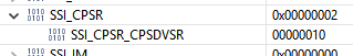
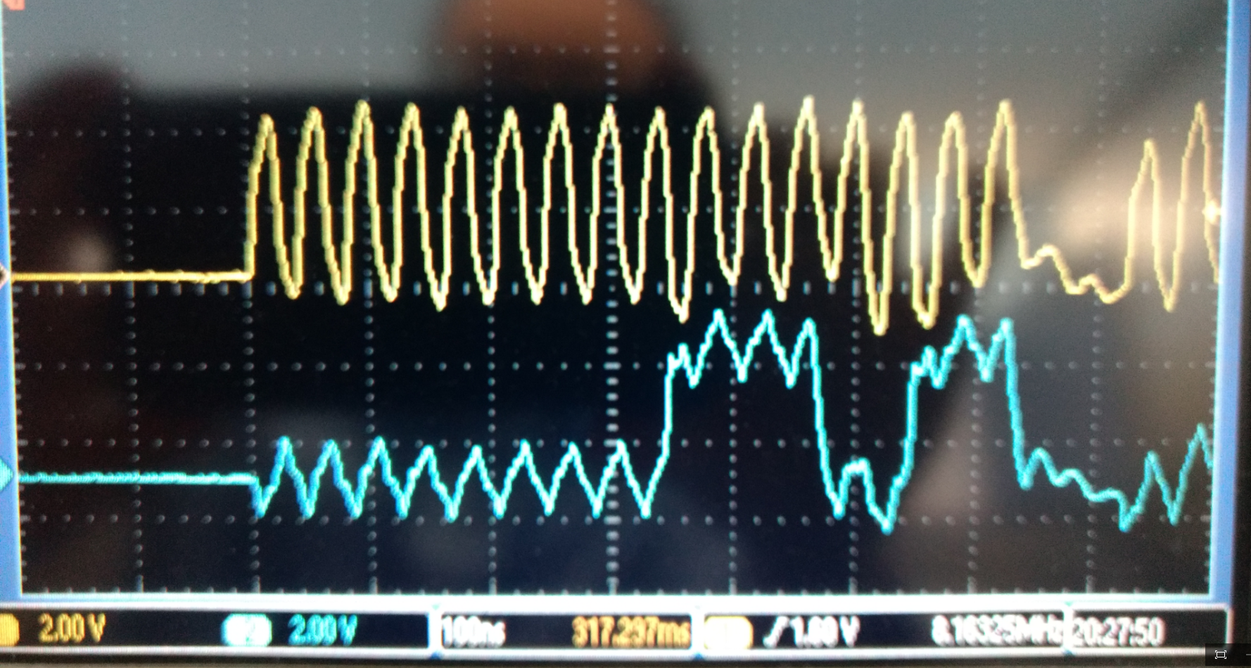
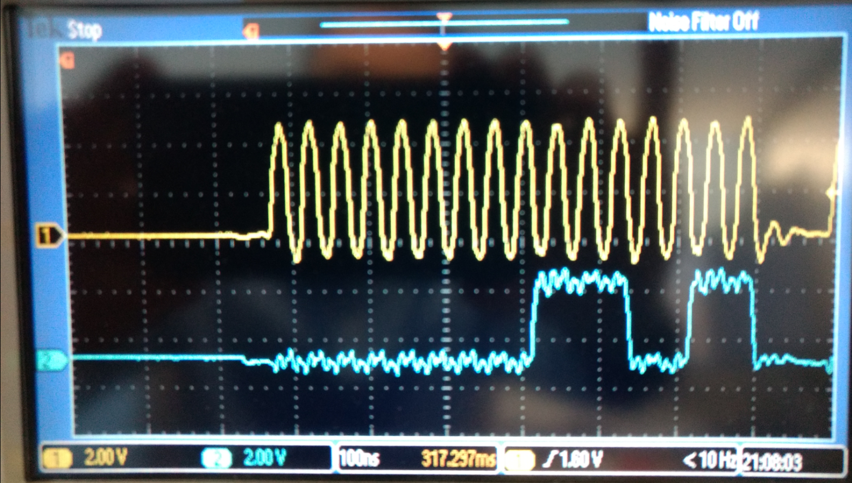
I want to have SPI clock in the range of 25 MHz using the PLL. I am using the following statements but am only getting a maximum of 10 MHz !

First I set the PLL clock frequency to insure it is more than double the required SPI clock as follows:

Setting the clocking to run at 100 MHz (200 MHz / 2) using the PLL.

SysCtlClockSet(SYSCTL_SYSDIV_2 | SYSCTL_USE_PLL | SYSCTL_OSC_MAIN | SYSCTL_XTAL_16MHZ);

Then setting the SPI clock to 20 MHz as follows:

SSIConfigSetExpClk(SSI3_BASE, SysCtlClockGet(), SSI_FRF_MOTO_MODE_0, SSI_MODE_MASTER, 20000000, 16);

Why do I get only 10 MHz?

Thanks,

Karim

  • Hi Karim,
    You cannot set the system clock to 100MHz as the TM4C123 only operates at max of 80MHz. Change to SYSCTL_SYSDIV_4 so the system clock is 50MHz and feed this clock to the SSI to generate the 25MHz SPI clock. However, this only limits your device frequency to 50MHz. If you want to operate at 80MHz for the device, then the closest SPICLK frequency you can get will be 20MHz.
  • Karim AbdelMoneim said:
    Setting the clocking to run at 100 MHz (200 MHz / 2) using the PLL.

    Max speed for the '123 devices is 80 MHz. I don't know what will happen when you ask for 100.

    Karim AbdelMoneim said:
    First I set the PLL clock frequency to insure it is more than double the required SPI clock as follows:

    The SPI rate can be at most 1/2 the System Clock. I would have called the VCO the PLL clock since that's what the PLL generates and it's fixed at 400MHz. The system clock is divided from that.

    Robert

  • Poster may have become confused by the difference between "123 and 129" - as the 129 employs a (potentially) faster system clock.
    As always - thorough read of the (chosen) MCU Manual is advised...

    It would have proved "advantageous" (perhaps required) for the "SysClock setting function" to have CAUGHT (and flagged) - that errant (over-speed) setting!

    It is noted that the "LIKE-less" yet (claimed) forum (upgrade?) has "induced another" into an "Incomprehensible/valueless" Subject/Head-Line!   (blind repetition of part number/IDE creates ZERO Drive/Interest...)

  • cb1_mobile said:
    Poster may have become confused by the difference between "123 and 129" - as the 129 employs a (potentially) faster system clock.
    As always - thorough read of the (chosen) MCU Manual is advised...

    It would also help if the TIVAWare manual indicated which combinations were invalid.

    cb1_mobile said:
    It would have proved "advantageous" (perhaps required) for the "SysClock setting function" to have CAUGHT (and flagged) - that errant (over-speed) setting!

    Even better if it could detect it at compile time. It should also catch the '123/'129 clash of functions, now some of that could be done at compile time.

    cb1_mobile said:
      (blind repetition of part number/IDE creates ZERO Drive/Interest...)

    Not sure it's retained the poster's interest either.

    Robert

  • Robert Adsett said:
    Not sure it's (blind repetition of part no./ide) retained the poster's interest either.

    At some point posters (will) require, quick/proper, "Attention from others" - and such (pardon) "valueless/fact-repeating Headlines" - are NOT (at all) informative - nor by any means, "drawing/motivating!"

    Many posts appear here - posters must expend some "thought/time/effort" in creating a "headline (subject)" which proves of (some) interest to others...   (i.e. some SELLING is required!)

  • Hi Charles,

    Thank you for the reply.

    I changed to 50 MHz for system clock as you advised, however using the following, am still getting only 10 MHz on the SPI clock;

    SysCtlClockSet(SYSCTL_SYSDIV_4 | SYSCTL_USE_PLL | SYSCTL_OSC_MAIN | SYSCTL_XTAL_16MHZ);

    SSIConfigSetExpClk(SSI3_BASE, SysCtlClockGet(), SSI_FRF_MOTO_MODE_0, SSI_MODE_MASTER, 20000000, 16);

    And also, could you please elaborate the relation between the maximum clock being 80 MHz and the PLL provided being 400 MHz, as shown in the block diagram?

    Regards,

    Karim

  • Karim AbdelMoneim said:
    I changed to 50 MHz for system clock as you advised, however using the following, am still getting only 10 MHz on the SPI clock;

    Can you show us a 'scope capture?

    Karim AbdelMoneim said:
    And also, could you please elaborate the relation between the maximum clock being 80 MHz

    The 80MHz is the maximum as specified in the data sheet (in the overview on page 38 and table 1.1. Table 5.6 is perhaps more explicit)

    Robert

  • Hello Robert,

    Thank you for the reply.

    Here is my scope picture, where am probing the SPI clock pin (PD0) as am using the SSI3 module.

    I also checked the corresponding registers for clock setting. As per the datasheet;

    SSI_Clk = SysClk / (CPSDVSR * (1+SCR)), where my CPSDVSR is currently 2 and SCR is zero! So giving an SSI_Clk that is SysClk/2 = 25 MHz.

    Thanks,

    Karim

  • May it be noted that should your board be a "LPad" - your choice of "PD0" is (particularly) unfortunate - as it is tied (directly) to PB6! (via a "famed" 0Ω "Plague-istor" (either R9 or R10). Now one would expect PB6 to exert (some) influence upon PD0 (poster's SPI clock) - yet "Cutting its output frequency - in HALF" - is beyond my (limited) understanding.

    Removal/DISCARD of (both) R9/R10 - should poster's board be an LPad - would serve as a "wise beginning!"

    It would also prove useful for poster to, "Switch to another SPI Port" (avoiding PD0/PD1) - and see if his set-up code (then) performs correctly...

    Many, many have "fallen to this trap" - yet vendor (finds the time) to "Kill LIKE" - while leaving R9 & R10 to continue (for years now) their mischief!

  • Hi Karim,
    You wrote SSIConfigSetExpClk(SSI3_BASE, SysCtlClockGet(), SSI_FRF_MOTO_MODE_0, SSI_MODE_MASTER, 20000000, 16). First of all, you specify 20MHz as the baud rate, not 25MHz. Secondly, can you please tell me what you get from SysCtlClockGet? I want to make sure it returns 50Mhz. I suggest you try below and let me know what you get on the scope.

    SSIConfigSetExpClk(SSI3_BASE, 50000000, SSI_FRF_MOTO_MODE_0, SSI_MODE_MASTER, 25000000, 16);
  • Hi Charles,

    Indeed - generating 20MHz "SPI Clk" from a 50MHz "SysClock" - may not be, "in the cards."     (not achievable - via "power of 2" integer divider)

    Are you in the camp that the "dead short" between PD0 & PB6 - by the "delightful" R9/R10 "devil pair" - may be "over-looked?"     (poster has noted his use of PD0 as SPI_CLK...even if PB6 is "unused" (for now) - when it "IS" switched to GPIO Output - dreaded "Output Contention" is invited - by the "primed/ready" devil pair...)

  • Hi cb1,
    I kind of doubt In this case. Karim should see SSI3CLK on both PD0 and PB6 as he didn't mention anything about using PB6 as a GPIO output. He can confirm this. From the scope, the SPICLK (aside from the wrong frequency) looks alright to me.
  • Thank you for the reply!

    I changed the SSI module i am using to SSI0 to avoid such vague connection with the 0 ohm resistor as you siggested. However still getting only maximum 10 MHz!

    Thanks,

    Karim

  • Hi Charles,

    I tried also the statement you suggested;
    SSIConfigSetExpClk(SSI3_BASE, 50000000, SSI_FRF_MOTO_MODE_0, SSI_MODE_MASTER, 25000000, 16);

    I still get maximum 10 MHz!

    I tried this on different SSI modules (SSI0/2/3) and I also tried on different board.

    Thanks,
    Karim
  • Bravo! Your "willingness" to experiment - especially w/an additional board - deserves applause! Firm/I have several such '123 LPads - is this what you are using? If so - we will "follow your foot-steps" - and report our findings!

    Kindly advise if you ARE using the '123 LPad! (and - it always proves advisable to "desolder & tombstone" each of the "devil pair" (resistors) - so their (ONGOING - vendor sanctioned) "torment" may be prevented. (such "sanction" is the truth - is it not?)

  • Hi Karim,
    Can you please paste your code?
  • Hi Cb1,

    Thanks for your help!
    Yes, am using the 123 LPads (Tiva™ C Series TM4C123G LaunchPad)

    Regards,
    Karim
  • Hi Charles,

    Following is my code.

    #include <stdio.h>
    #include <stdint.h>
    #include <stdbool.h>
    #include "inc/hw_types.h"
    #include "inc/hw_memmap.h"
    #include "driverlib/sysctl.h"
    #include "driverlib/gpio.h"
    #include "driverlib/pin_map.h"
    #include "driverlib/uart.h"
    #include "utils/uartstdio.h"
    #include "driverlib/ssi.h"
    #include "utils/uartstdio.h"
    #include "driverlib/adc.h"

    #define NUM_SSI_DATA 3

    uint32_t pui32DataTx[NUM_SSI_DATA];
    uint32_t pui32DataRx[NUM_SSI_DATA];

    SPI_Init()
    {
    //
    // Set the clocking to run at 50 MHz (200 MHz / 4) using the PLL.
    //
    SysCtlClockSet(SYSCTL_SYSDIV_4 | SYSCTL_USE_PLL | SYSCTL_OSC_MAIN |
    SYSCTL_XTAL_16MHZ);

    //
    // Enable SSI peripheral.
    //
    SysCtlPeripheralEnable(SYSCTL_PERIPH_SSI0);

    //
    // Enable GPIO A Peripheral for SSI0 Module.
    //
    SysCtlPeripheralEnable(SYSCTL_PERIPH_GPIOA);

    //
    // Configure the SSI0 functionality for GPIO A pins.
    //
    GPIOPinConfigure(GPIO_PA2_SSI0CLK);
    GPIOPinConfigure(GPIO_PA3_SSI0FSS);
    GPIOPinConfigure(GPIO_PA4_SSI0RX);
    GPIOPinConfigure(GPIO_PA5_SSI0TX);

    //
    // SSI0 Pin Assignment
    //
    GPIOPinTypeSSI(GPIO_PORTA_BASE, GPIO_PIN_5 | GPIO_PIN_4 | GPIO_PIN_3 |
    GPIO_PIN_2);

    //
    // SSI0 Clock Configuration
    //
    SSIConfigSetExpClk(SSI0_BASE, 50000000, SSI_FRF_MOTO_MODE_0, SSI_MODE_MASTER, 25000000, 16);

    //
    // Enable SSI0 module.
    //
    SSIEnable(SSI0_BASE);
    }

    //
    // The following function puts an incremental value on the Tx pin of the SSI module to be received by a DAC with SPI interface.
    // I am not receiving any signals from the DAC interface, so am not using the receive pin of the SSI module (Wire is disconnected).
    // Tha maximum frequency that can be handled by the DAC SPI interface is 30 MHz.

    void FreqSweep()
    {
    static int val = 20;
    pui32DataTx[0] = val;

    while(SSIDataGetNonBlocking(SSI0_BASE, &pui32DataRx[0])){}

    SSIDataPut(SSI0_BASE, pui32DataTx[0]);

    // Frequency Sweep
    if (val < 7535)
    val += 20;
    else
    val = 20;

    while(SSIBusy(SSI0_BASE)){}
    }


    Regards,
    Karim
  • It is preferred that you insert (some) delay prior to, and after, calling each, "SysCtlPeripheralEnable()" function.     You may optionally (even better) call the appropriate, "Peripheral Ready" function.

    I suggest that you RESET the SSI Function prior to ANY set-up/config - just to be on the SAFE SIDE!

    You are (almost) there - stay stong!

  • Try the attached example with ssi0 running at 25MHz.

    //*****************************************************************************
    //
    // spi_master.c - Example demonstrating how to configure SSI0 in SPI master
    //                mode.
    //
    // Copyright (c) 2010-2016 Texas Instruments Incorporated.  All rights reserved.
    // Software License Agreement
    // 
    //   Redistribution and use in source and binary forms, with or without
    //   modification, are permitted provided that the following conditions
    //   are met:
    // 
    //   Redistributions of source code must retain the above copyright
    //   notice, this list of conditions and the following disclaimer.
    // 
    //   Redistributions in binary form must reproduce the above copyright
    //   notice, this list of conditions and the following disclaimer in the
    //   documentation and/or other materials provided with the  
    //   distribution.
    // 
    //   Neither the name of Texas Instruments Incorporated nor the names of
    //   its contributors may be used to endorse or promote products derived
    //   from this software without specific prior written permission.
    // 
    // THIS SOFTWARE IS PROVIDED BY THE COPYRIGHT HOLDERS AND CONTRIBUTORS
    // "AS IS" AND ANY EXPRESS OR IMPLIED WARRANTIES, INCLUDING, BUT NOT
    // LIMITED TO, THE IMPLIED WARRANTIES OF MERCHANTABILITY AND FITNESS FOR
    // A PARTICULAR PURPOSE ARE DISCLAIMED. IN NO EVENT SHALL THE COPYRIGHT
    // OWNER OR CONTRIBUTORS BE LIABLE FOR ANY DIRECT, INDIRECT, INCIDENTAL,
    // SPECIAL, EXEMPLARY, OR CONSEQUENTIAL DAMAGES (INCLUDING, BUT NOT
    // LIMITED TO, PROCUREMENT OF SUBSTITUTE GOODS OR SERVICES; LOSS OF USE,
    // DATA, OR PROFITS; OR BUSINESS INTERRUPTION) HOWEVER CAUSED AND ON ANY
    // THEORY OF LIABILITY, WHETHER IN CONTRACT, STRICT LIABILITY, OR TORT
    // (INCLUDING NEGLIGENCE OR OTHERWISE) ARISING IN ANY WAY OUT OF THE USE
    // OF THIS SOFTWARE, EVEN IF ADVISED OF THE POSSIBILITY OF SUCH DAMAGE.
    // 
    // This is part of revision 2.1.3.156 of the Tiva Firmware Development Package.
    //
    //*****************************************************************************
    
    #include <stdbool.h>
    #include <stdint.h>
    #include "inc/hw_memmap.h"
    #include "driverlib/gpio.h"
    #include "driverlib/pin_map.h"
    #include "driverlib/ssi.h"
    #include "driverlib/sysctl.h"
    #include "driverlib/uart.h"
    #include "driverlib/rom_map.h"
    #include "driverlib/rom.h"
    #include "utils/uartstdio.h"
    
    
    //*****************************************************************************
    //
    //! \addtogroup ssi_examples_list
    //! <h1>SPI Master (spi_master)</h1>
    //!
    //! This example shows how to configure the SSI0 as SPI Master.  The code will
    //! send three characters on the master Tx then polls the receive FIFO until
    //! 3 characters are received on the master Rx.
    //!
    //! This example uses the following peripherals and I/O signals.  You must
    //! review these and change as needed for your own board:
    //! - SSI0 peripheral
    //! - GPIO Port A peripheral (for SSI0 pins)
    //! - SSI0Clk - PA2
    //! - SSI0Fss - PA3
    //! - SSI0Rx  - PA4
    //! - SSI0Tx  - PA5
    //!
    //! The following UART signals are configured only for displaying console
    //! messages for this example.  These are not required for operation of SSI0.
    //! - UART0 peripheral
    //! - GPIO Port A peripheral (for UART0 pins)
    //! - UART0RX - PA0
    //! - UART0TX - PA1
    //!
    //! This example uses the following interrupt handlers.  To use this example
    //! in your own application you must add these interrupt handlers to your
    //! vector table.
    //! - None.
    //
    //*****************************************************************************
    
    //*****************************************************************************
    //
    // Number of bytes to send and receive.
    //
    //*****************************************************************************
    #define NUM_SSI_DATA            3
    
    //*****************************************************************************
    //
    // This function sets up UART0 to be used for a console to display information
    // as the example is running.
    //
    //*****************************************************************************
    void
    InitConsole(void)
    {
        //
        // Enable GPIO port A which is used for UART0 pins.
        // TODO: change this to whichever GPIO port you are using.
        //
        SysCtlPeripheralEnable(SYSCTL_PERIPH_GPIOA);
    
        //
        // Configure the pin muxing for UART0 functions on port A0 and A1.
        // This step is not necessary if your part does not support pin muxing.
        // TODO: change this to select the port/pin you are using.
        //
        GPIOPinConfigure(GPIO_PA0_U0RX);
        GPIOPinConfigure(GPIO_PA1_U0TX);
    
        //
        // Enable UART0 so that we can configure the clock.
        //
        SysCtlPeripheralEnable(SYSCTL_PERIPH_UART0);
    
        //
        // Use the internal 16MHz oscillator as the UART clock source.
        //
        UARTClockSourceSet(UART0_BASE, UART_CLOCK_PIOSC);
    
        //
        // Select the alternate (UART) function for these pins.
        // TODO: change this to select the port/pin you are using.
        //
        GPIOPinTypeUART(GPIO_PORTA_BASE, GPIO_PIN_0 | GPIO_PIN_1);
    
        //
        // Initialize the UART for console I/O.
        //
        UARTStdioConfig(0, 115200, 16000000);
    
    }
    
    //*****************************************************************************
    //
    // Configure SSI0 in master Freescale (SPI) mode.  This example will send out
    // 3 bytes of data, then wait for 3 bytes of data to come in.  This will all be
    // done using the polling method.
    //
    //*****************************************************************************
    int
    main(void)
    {
    #if defined(TARGET_IS_TM4C129_RA0) ||                                         \
        defined(TARGET_IS_TM4C129_RA1) ||                                         \
        defined(TARGET_IS_TM4C129_RA2)
        uint32_t ui32SysClock;
    #endif
    
        uint32_t pui32DataTx[NUM_SSI_DATA];
        uint32_t pui32DataRx[NUM_SSI_DATA];
        uint32_t ui32Index;
    
        //
        // Set the clocking to run directly from the external crystal/oscillator.
        // TODO: The SYSCTL_XTAL_ value must be changed to match the value of the
        // crystal on your board.
        //
    #if defined(TARGET_IS_TM4C129_RA0) ||                                         \
        defined(TARGET_IS_TM4C129_RA1) ||                                         \
        defined(TARGET_IS_TM4C129_RA2)
        ui32SysClock = MAP_SysCtlClockFreqSet((SYSCTL_XTAL_25MHZ |
                                           SYSCTL_OSC_MAIN |
                                           SYSCTL_USE_OSC), 25000000);
    #else
        SysCtlClockSet(SYSCTL_SYSDIV_4 | SYSCTL_USE_PLL | SYSCTL_OSC_MAIN |
                       SYSCTL_XTAL_16MHZ);
    #endif
    
        //
        // Set up the serial console to use for displaying messages.  This is
        // just for this example program and is not needed for SSI operation.
        //
        InitConsole();
    
        //
        // Display the setup on the console.
        //
        UARTprintf("SSI ->\n");
        UARTprintf("  Mode: SPI\n");
        UARTprintf("  Data: 8-bit\n\n");
    
        //
        // The SSI0 peripheral must be enabled for use.
        //
        ROM_SysCtlPeripheralEnable(SYSCTL_PERIPH_SSI0);
    
        //
        // For this example SSI0 is used with PortA[5:2].  The actual port and pins
        // used may be different on your part, consult the data sheet for more
        // information.  GPIO port A needs to be enabled so these pins can be used.
        // TODO: change this to whichever GPIO port you are using.
        //
        SysCtlPeripheralEnable(SYSCTL_PERIPH_GPIOA);
    
        //
        // Configure the pin muxing for SSI0 functions on port A2, A3, A4, and A5.
        // This step is not necessary if your part does not support pin muxing.
        // TODO: change this to select the port/pin you are using.
        //
        GPIOPinConfigure(GPIO_PA2_SSI0CLK);
        GPIOPinConfigure(GPIO_PA3_SSI0FSS);
        GPIOPinConfigure(GPIO_PA4_SSI0RX);
        GPIOPinConfigure(GPIO_PA5_SSI0TX);
    //      GPIOPinConfigure(GPIO_PA4_SSI0XDAT0);
    //      GPIOPinConfigure(GPIO_PA5_SSI0XDAT1);
    
    
        //
        // Configure the GPIO settings for the SSI pins.  This function also gives
        // control of these pins to the SSI hardware.  Consult the data sheet to
        // see which functions are allocated per pin.
        // The pins are assigned as follows:
        //      PA5 - SSI0Tx
        //      PA4 - SSI0Rx
        //      PA3 - SSI0Fss
        //      PA2 - SSI0CLK
        // TODO: change this to select the port/pin you are using.
        //
        GPIOPinTypeSSI(GPIO_PORTA_BASE, GPIO_PIN_5 | GPIO_PIN_4 | GPIO_PIN_3 |
                       GPIO_PIN_2);
    
        //
        // Configure and enable the SSI port for SPI master mode.  Use SSI0,
        // system clock supply, idle clock level low and active low clock in
        // freescale SPI mode, master mode, 1MHz SSI frequency, and 8-bit data.
        // For SPI mode, you can set the polarity of the SSI clock when the SSI
        // unit is idle.  You can also configure what clock edge you want to
        // capture data on.  Please reference the datasheet for more information on
        // the different SPI modes.
        //
    #if defined(TARGET_IS_TM4C129_RA0) ||                                         \
        defined(TARGET_IS_TM4C129_RA1) ||                                         \
        defined(TARGET_IS_TM4C129_RA2)
        SSIConfigSetExpClk(SSI0_BASE, ui32SysClock, SSI_FRF_MOTO_MODE_0,
                           SSI_MODE_MASTER, 1000000, 8);
    #else
        uint32_t freq = 0;
        freq = SysCtlClockGet();
        SSIConfigSetExpClk(SSI0_BASE, freq, SSI_FRF_MOTO_MODE_0,
                           SSI_MODE_MASTER, 25000000, 16);
    #endif
    
        //
        // Enable the SSI0 module.
        //
        SSIEnable(SSI0_BASE);
    
        //
        // Read any residual data from the SSI port.  This makes sure the receive
        // FIFOs are empty, so we don't read any unwanted junk.  This is done here
        // because the SPI SSI mode is full-duplex, which allows you to send and
        // receive at the same time.  The SSIDataGetNonBlocking function returns
        // "true" when data was returned, and "false" when no data was returned.
        // The "non-blocking" function checks if there is any data in the receive
        // FIFO and does not "hang" if there isn't.
        //
        while(SSIDataGetNonBlocking(SSI0_BASE, &pui32DataRx[0]))
        {
        }
    
        //
        // Initialize the data to send.
        //
        pui32DataTx[0] = 's';
        pui32DataTx[1] = 'p';
        pui32DataTx[2] = 'i';
    
    while (1) {
        //
        // Display indication that the SSI is transmitting data.
        //
    //    UARTprintf("Sent:\n  ");
    
        //
        // Send 3 bytes of data.
        //
        for(ui32Index = 0; ui32Index < NUM_SSI_DATA; ui32Index++)
        {
            //
            // Display the data that SSI is transferring.
            //
      //      UARTprintf("'%c' ", pui32DataTx[ui32Index]);
    
            //
            // Send the data using the "blocking" put function.  This function
            // will wait until there is room in the send FIFO before returning.
            // This allows you to assure that all the data you send makes it into
            // the send FIFO.
            //
            SSIDataPut(SSI0_BASE, pui32DataTx[ui32Index]);
        }
    
        //
        // Wait until SSI0 is done transferring all the data in the transmit FIFO.
        //
        while(SSIBusy(SSI0_BASE))
        {
        }
    
        //
        // Display indication that the SSI is receiving data.
        //
        //UARTprintf("\nReceived:\n  ");
    
        //
        // Receive 3 bytes of data.
        //
        for(ui32Index = 0; ui32Index < NUM_SSI_DATA; ui32Index++)
        {
            //
            // Receive the data using the "blocking" Get function. This function
            // will wait until there is data in the receive FIFO before returning.
            //
            SSIDataGet(SSI0_BASE, &pui32DataRx[ui32Index]);
    
            //
            // Since we are using 8-bit data, mask off the MSB.
            //
            pui32DataRx[ui32Index] &= 0x00FF;
    
            //
            // Display the data that SSI0 received.
            //
          //  UARTprintf("'%c' ", pui32DataRx[ui32Index]);
        }
    }
    
        //
        // Return no errors
        //
        return(0);
    }
    

    I ran this example and the scope shows the SPICLK is 25Mhz. My timescale is 100ns per division and you see about 2.5 clocks in each division.

    Below is the zoom in view with the measurement of the clock and it shows 40ns. 

  • Charles,

    At such speed - the waveform may better reveal if the (assumed) scope's (~3") ground probe (lead) is removed - and a (minimal length) "grounded wire-loop" instead - directly attaches (encircles) the probe's metallic body.

  • Hi cb1,
    You are exactly right. I forgot to connect the probe ground on the TX pin (the bottom signal). :-)
  • It is, nonetheless, a good illustration of why these signals should not be treated lightly once you approach these speeds Charles. SPI requires that the data be stable during the clock rise and fall.

    Robert
  • Hi Robert,

     I agree. Here is scope shot after proper grounding.  I have the TX/RX tied together and the receiver is receiving the data correctly.

  • Hello Charles,

    Your code allowed me to go further with the troubleshooting. I realized that my SPI code was working correctly giving the same results as your code.

    Which got me thinking towards the code in the "main". I was using the ADC module as well for some signal conversion. However, I was not setting its SysClk with the same frequency as for the SPI (PLL at 50 MHz) and that was the conflict!

    Once I corrected this, I got the nice 25 MHz from the SPI clk on the scope.

    Thank you a lot Charles for the support! And many thanks to Robert and cb1 for your contribution, advice and support!

    Regards,

    Karim

  • Hi Karim,
    Glad your problem is solved. Why would you want to configure the system clock frequency inside each peripheral's initialization? You should initialize the device (i.e. device feq) before you initialize other peripherals.
  • It is unlikely that any of the "forum helper group" would have been able to resolve such an issue - as the, "Alteration of System Clock" (as Charles rightly) "PC be damned" (almost) protests - proves extremely unexpected!

    Lesson learned here is that we must broaden our diagnosis - thus beware of - perhaps even "expect" - the unexpected! Any "unexplained deviation from the norm" must bring about "poster admission" of "any/all" modifications (such as Sys Clock, here) which may influence the outcome...
  • Yes, you are absolutely right! I now learned that I should have one time clock initialization for the whole device.

    Thanks,
    Karim
  • Sorry for the inconvenience! :D
  • No sorrow sought nor required.        

    There IS a clear lesson to be learned here - and the combined diagnostic efforts of (3 helpers) failed to, "Ascertain if (any) of the MCU's frequency control mechanisms were subject to change and/or adjustment."    While that's a (bit) unusual/unexpected - it should have been questioned - and if not (now) properly memorialized & recorded here - may be repeated.

    It is true that "helpers" may, "Learn/Benefit as much as those they assist" - but (only) if the "real pivot/trigger issue" - is properly identified - and brought to the surface - so that it proves, "not" repeated...     (my writing attempts to "tie the bow" upon "your discovery of the issue" - which the "helper crüe" should have "prompted for & detected" - and did not!)      

    Learning, "How a mistake was made" may prove (even) more important than the "mistake itself" - as this may identify an imperfect "technique" - which if not "corrected" - is likely to repeat!      (as seen so often here - R9/R10 continue their (unwanted) poster-distressing onslaught - absolutely unabated - while "LIKE" receives (unnecessary/destructive) attention!)     Ignoring an error ... proves FAR from correcting... Pity...

  • cb1_mobile said:
    Learning, "How a mistake was made" may prove (even) more important than the "mistake itself" - as this may identify an imperfect "technique" - which if not "corrected" - is likely to repeat!

    That is in fact an interesting point of view! A true lesson learner, I totally agree!

  • And - I was NOT alone in recognizing that you were "smart/motivated sufficiently" to "recognize, benefit from & incorporate/adopt" this truth!

    This type of, "on-going, operational conclusion" is one which most "rushed forum responses" gloss over - thus impeding, "Lesson Learned!"      

    This "generalization" - from a "Singular solution" - into a far more powerful/useful/re-usable, "General Solution METHOD" - substantially raises "problem-solving capability & efficiency" - and should be a "sought objective" - for each/every challenge...