This thread has been locked.

If you have a related question, please click the "Ask a related question" button in the top right corner. The newly created question will be automatically linked to this question.

TM4C1237H6PGE: Error connecting to the target: (Error -1170 @ 0x0) Unable to access the DAP.

Part Number: TM4C1237H6PGE
Other Parts Discussed in Thread: SEGGER, UNIFLASH

Hi

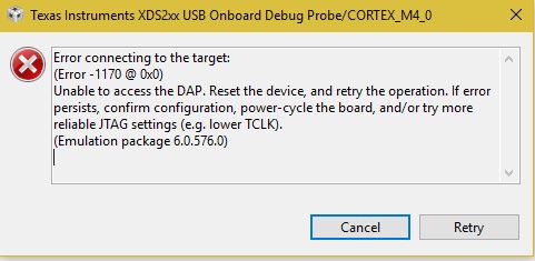
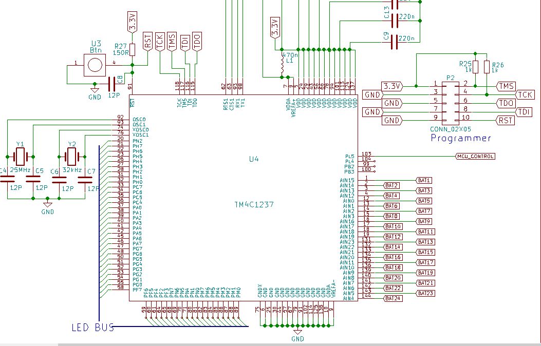
I am in desperate need of assistance with launching the debugger on CCSv7 using an XDS200. I have made a custom board using the TM4C1237H6PGE. When I do the integrity test it is successful but when i launch the debugger i get the following error "Error connecting to the target: (Error -1170 @ 0x0) Unable to access the DAP.". I have built another board before using the TM4C1294 which worked on the first try. I have tried a different programmer checked connections thoroughly and tried a different PC with none solving the problem. Below I have added the Integrity test, the error that appears and my schematic.

Thanks for your assistance.

----------------------------------------------------------------------------------------------------------------------------------------------

[Start]

Execute the command:

%ccs_base%/common/uscif/dbgjtag -f %boarddatafile% -rv -o -S integrity

[Result]


-----[Print the board config pathname(s)]------------------------------------

C:\Users\Pranav\AppData\Local\TEXASI~1\CCS\
ti\0\0\BrdDat\testBoard.dat

-----[Print the reset-command software log-file]-----------------------------

This utility has selected a 560/2xx-class product.
This utility will load the program 'xds2xxu.out'.
The library build date was 'Feb 13 2017'.
The library build time was '15:28:48'.
The library package version is '6.0.576.0'.
The library component version is '35.35.0.0'.
The controller does not use a programmable FPGA.
The controller has a version number of '13' (0x0000000d).
The controller has an insertion length of '0' (0x00000000).
This utility will attempt to reset the controller.
This utility has successfully reset the controller.

-----[Print the reset-command hardware log-file]-----------------------------

This emulator does not create a reset log-file.

-----[Perform the Integrity scan-test on the JTAG IR]------------------------

This test will use blocks of 64 32-bit words.
This test will be applied just once.

Do a test using 0xFFFFFFFF.
Scan tests: 1, skipped: 0, failed: 0
Do a test using 0x00000000.
Scan tests: 2, skipped: 0, failed: 0
Do a test using 0xFE03E0E2.
Scan tests: 3, skipped: 0, failed: 0
Do a test using 0x01FC1F1D.
Scan tests: 4, skipped: 0, failed: 0
Do a test using 0x5533CCAA.
Scan tests: 5, skipped: 0, failed: 0
Do a test using 0xAACC3355.
Scan tests: 6, skipped: 0, failed: 0
All of the values were scanned correctly.

The JTAG IR Integrity scan-test has succeeded.

-----[Perform the Integrity scan-test on the JTAG DR]------------------------

This test will use blocks of 64 32-bit words.
This test will be applied just once.

Do a test using 0xFFFFFFFF.
Scan tests: 1, skipped: 0, failed: 0
Do a test using 0x00000000.
Scan tests: 2, skipped: 0, failed: 0
Do a test using 0xFE03E0E2.
Scan tests: 3, skipped: 0, failed: 0
Do a test using 0x01FC1F1D.
Scan tests: 4, skipped: 0, failed: 0
Do a test using 0x5533CCAA.
Scan tests: 5, skipped: 0, failed: 0
Do a test using 0xAACC3355.
Scan tests: 6, skipped: 0, failed: 0
All of the values were scanned correctly.

The JTAG DR Integrity scan-test has succeeded.

[End]

----------------------------------------------------------------------------------------------------------------

  • Hi,
    Can you compare your current board (with TM4C1237 device) with the other working board (with TM4C1294) and see what is the difference?

    I will suggest you check the following.

    1. Check if TM4C device is under reset. Please check the Reset Pin and the VDDC pin. The former should be at 3.3V and the latter at 1.2V if VDD and VDDA are proper 3.3V
    2. Power up the board and check the TDO pin using a scope. Does it show a 15-20 Hz wave?

    As you can do proper scan on the scan chain, it leads me to believe you didn't have swapped JTAG pins. We can isolate this as a cause.

    Please also refer to to this app note section 3 on the JTAG interface. www.ti.com/.../spma075.pdf
  • And - if I may - might you add a pull-up R to TDI (pin 8 - your P2).     We note the use of 1K for pull-ups - that's bit too low in value, IMO.    (suggest 3K3-4K7 instead.)    

    Connection into your P2 should be as short as possible.

    These guides have "recovered" multiple of our clients' boards - suffering as you report.    (and - while "blasphemy" here - your use of Segger's "J-Link" (a proven, superior JTAG/SWD Probe) often, "restores order!")

  • Thanks for the reply!

    I have not had any success i am still getting Error 1170!

    I have done all the recommendations that you have mentioned above.

    I have replaced all the pull up resistors with higher resistance. 

    The TDO line has been tied to VCC with a pull up resistor.

    The VDDA and VDD are at a steady 3.3V with 0 to 40mV ripple.

    The VDDC line has a ripple of 1V and an avg of 1.5V.

    Comparing the 2 custom boards they are identical.

    I have even made 2 boards incase 1 was a defect and tried a bench power supply to eliminate the onboard powersupply

  • Pranav,
    Your VDDC line is definitely wrong. It suggests something wrong on your soldering, or even in your power circuit...
    The VDDA is also tricky, as you have an inductor and a trace going up to "unkown"... If VDDA is not ready when you power your MCU with VDDC, it will lock. In some designs, we actually use the VDDA signal as the enabler to the VDDC power switcher! Try to visualize the ramp up on both lines.
    Is there software in your MCU? Can you confirm it is running? If a temporary situation locked your device, you might need to unlock it using LMFlash.
    Regards
    Bruno
  • Thanks for the reply Bruno.
    I am checking the VDDC line now.
    There is no software on the MCU.
    The VDDA pin is connected to 3.3V via an inductor and also to ground via a 220nF cap.
    Regards Pranav
  • How would I unlock it using LMFlasher and the xds200?
  • I'm not into performing calculations to see if your VDDA will ramp fast enough, but again, did you look it in a scope? It would be more correct to power VDDA before the digital supply, not after.

    I don't recall if LMFlash can unlock using the XDS200 - maybe you will need to use the ICDI of a Launchpad for that. Give it a try with UniFlash also (if the unlock option is not there for your debugger, then that combination can't be used).
  • You cannot use LM flash programmer to unlock the device using xds200. Please refer to section 5.3.2 of this app note to unlock when xds200 is used. The utility is dbgjtag.exe. With that said, unlock is meaningful if you have some destructive code in the flash already. In your case, this is not the cause. You want to understand your power supply issue first.
  • Pranav Sewpersad said:
    The VDDC line has a ripple of 1V and an avg of 1.5V.

    Has this amount of ripple been noted?      Can this be "normal?"        I would hazard the guess that the "Caps on this line are inadequate" - should that degree of ripple be present.      Caps on VDDC MUST be as the manual specifies - I suspect "mismarked or installed incorrectly!"

    This is one area for focus - any custom board brings  with it MANY areas demanding such focus...      And never/ever is the need for custom (and the headaches resulting) described...    LPad into user's special function board - proves a "far more likely" road to success...

  • Thanks for all the replies.
    I have solved the power supply issues and replaced the the MCU all the power lines are acting as required and have removed all other circuitry from the board. All that is on the board is the MCU with all the specified capacitors and the Jtag circuitry.
    I am still getting the same error and have no clue where to look for errors.
    Is it possible that the XDS200 is incompatible with the TM4C1237H6PGE?
  • The board is being powered by a standard bench power supply
  • Even after several viewing attempts - I cannot find,  "VDDC" on your schematic.      The capacitive treatment of that pin is critical - the MCU manual's specification MUST be followed.

    Is it not noteworthy that your,  "JTAG Probe"  reports  BOTH  Success and then FAILURE?     How can that be?

    Kindly scope the (past) WORKING board - ideally obrtaining a,  "Scope Cap" of VDDC.       Then - repeat that process on (both) of your (new) FAILING boards - and present both Scope Caps (of VDDC) - clearly identified/linked to each board.    (Good board  AND  Bad board "VDDC Scope Caps" (BOTH) - placed closely - one atop the other - same scope set-up/scales etc!)

    Your schematic - possibly due to "drawing ease" - reveals JUST 2 Caps upon VDD.     MANY such (lower value) caps ARE required - placed (at least) at  "every other"  VDD pin - and in close proximity to the MCU.    Have you - instead - employed just two caps - as your schematic suggests?

    The ripple voltage you report (1V - iirc)  FAR exceeds that upon ANY of our working boards.     (suggesting:  mismarked, under-valued, or failed Capacitor connections to MCU's VDDC pin!)

    STILL though - the "disputed & conflicting findings" of your tool ...  SCREAMS  "Tool as Amateur" - does it not?      Why is this fact avoided?     (such has been reported here - repeatedly - always DUCKED!)   "Avoidance does not qualify as a Solution!"

  • The schematic uploaded is the initial schematic, I have added the caps for the VDDC on to the board and I am now getting a stable 1.2V with a 150mV ripple.

    I also don't understand the success failure.

    The previous boards I spoke about have the TM4c1294 MCU.

    There are VDD caps close to all the VDD pins of the MCU when I took the screen shot they have been cut out.

    I have put the scope on all the JTAG pins of the board with the TM4C1294 (working board) and compared it to the board with the Tm4C1237 (not working) and have noticed that the TDO and TDI pins on the board that is not working don't show data transmission.
  • So - this (very) early morning diagnosis has borne fruit - has it not?

    VDDC was proven to be "well diagnosed" - WAS incorrectly implemented! On several (past) occasions - that mistake (No or insufficient caps) had "KILLED" client boards! It is likely - just as your schematic revealed - that NO Caps appeared (earlier) upon VDDC - which cannot be good! (your MCU may have been damaged - proper "ripple now" - does not insure its survival)

    How many Caps appear upon your VDD pins - you've made no mention - it is suspected that you've deployed just TWO. That's correct - is it not?

    Earlier you noted "Two new boards" were produced. Do both (really) show "No Activity" upon TDO & TDI - really? Scope CAP was requested - we NEED to SEE levels - undescribed - your report...

  • I have got it working.

    Removed all the caps from VDDC (leaving it unconnected).
    I needed to unlock the MCUs using Lmflasher and a lauchpad.
    All the MCUs that I received from TI seems locked is there a reason or is this a fault?
    Now I can flash using the XDS.


    Thanks for your replies.
  • HI Pranav,
    Glad that it is working now but I'm still confused how you got it working compared to your original non-working setup. You need to have proper filter cap on the VDDC. Please refer to the datasheet for minimum filter cap on the LDO supply which is 2.5uF. Even you got it working without the any cap on the VDDC but by no means it will work in your application. The chip switching activities can create ripple on the power supply which can lead the chip to operate out of spec.

  • Poster's "SELF AWARDED VERIFY" which proves "Ever so Wrong" (REMOVE ALL CAPS FROM VDDC) - Likely TO CAUSE "DEATH" TO MCUs of  readers landing here  -  who may "follow"  THIS (Horrid)  "Award of Verify!"  

    Highly DESTRUCTIVE!