This thread has been locked.

If you have a related question, please click the "Ask a related question" button in the top right corner. The newly created question will be automatically linked to this question.

TM4C123GH6PM: problem with ssi communication

Part Number: TM4C123GH6PM
Other Parts Discussed in Thread: EK-TM4C123GXL

hi everyone,

I just started working with micro-controllers. I'm using the TM4C123GH6PM.

I haven't used ssi communication so far, so i wrote the attached code, in which the controller sends messages to itself via two ssi ports.

I simplified the program by allowng only OT interrupts, for now.

When I run this code, the receiving port calls the ISR and saves the data sent, than it is called one more time, but writes no data, and no longer calls the ISR.

Am I missing something?

#include <stdint.h>
#include <stdbool.h>
#include "inc/hw_memmap.h"
#include "inc/hw_ints.h"
#include "driverlib/debug.h"
#include "driverlib/ssi.h"
#include "driverlib/sysctl.h"
#include "driverlib/gpio.h"
#include "driverlib/pin_map.h"

#define BUFFER_SIZE 256

uint8_t message_Index = 0 ;
uint32_t dataReceived[BUFFER_SIZE] = {0} ;

void SSI2ReceiveISR (void)
{
    SSIIntClear(SSI2_BASE, SSI_RXTO) ;
    SSIDataGetNonBlocking(SSI2_BASE, &dataReceived[message_Index++]) ;
}


int main(void)
{
    volatile uint32_t cyclic_Counter = 0 ;

    // enable ssi1 peripheral:
    SysCtlPeripheralEnable(SYSCTL_PERIPH_SSI1);
    while(!SysCtlPeripheralReady(SYSCTL_PERIPH_SSI1))
    {
    }

    // enable ssi2 peripheral:
    SysCtlPeripheralEnable(SYSCTL_PERIPH_SSI2);
    while(!SysCtlPeripheralReady(SYSCTL_PERIPH_SSI2))
    {
    }

    //
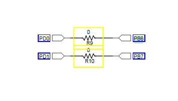
    // For this example SSI0 is used with PortA[5:2].  The actual port and
    // pins used may be different on your part, consult the data sheet for
    // more information.  GPIO port A needs to be enabled so these pins can
    // be used.
    //
    SysCtlPeripheralEnable(SYSCTL_PERIPH_GPIOB) ;
    SysCtlPeripheralEnable(SYSCTL_PERIPH_GPIOD) ;

    //
    // Configure the pin for SSI's
    GPIOPinConfigure(GPIO_PD0_SSI1CLK);
    GPIOPinConfigure(GPIO_PD1_SSI1FSS);
    GPIOPinConfigure(GPIO_PD2_SSI1RX);
    GPIOPinConfigure(GPIO_PD3_SSI1TX);

    GPIOPinConfigure(GPIO_PB4_SSI2CLK);
    GPIOPinConfigure(GPIO_PB5_SSI2FSS);
    GPIOPinConfigure(GPIO_PB6_SSI2RX);
    GPIOPinConfigure(GPIO_PB7_SSI2TX);

     //
     // Configure the GPIO settings for the SSI pins.
     // see which functions are allocated per pin.
     // The pins are assigned as follows:
     //      PB4 - SSI2CLK
     //      PB5 - SSI2FSS
     //      PB6 - SSI2RX
     //      PB7 - SSI2TX
     //      PD0 - SSI1CLK
     //      PD1 - SSI1FSS
     //      PD2 - SSI1RX
     //      PD3 - SSI1TX
     //
     GPIOPinTypeSSI(GPIO_PORTB_BASE, GPIO_PIN_4 | GPIO_PIN_5 | GPIO_PIN_6 |
                                     GPIO_PIN_7 );

     GPIOPinTypeSSI(GPIO_PORTD_BASE, GPIO_PIN_0 | GPIO_PIN_1 | GPIO_PIN_2 |
                                     GPIO_PIN_3 );

    //configuring the two ssi's, 1 as a master and 2 as a slave
    SSIConfigSetExpClk(SSI1_BASE, SysCtlClockGet(), SSI_FRF_MOTO_MODE_0, SSI_MODE_MASTER, 500000, 8) ;
    SSIConfigSetExpClk(SSI2_BASE, SysCtlClockGet(), SSI_FRF_MOTO_MODE_0, SSI_MODE_SLAVE, 500000, 8) ;

    // enabling the two ssi's
    SSIEnable(SSI1_BASE) ;
    SSIEnable(SSI2_BASE) ;

    // for the receiver port, we allow only time out interrupts, or full\half-full FIFO interrupts
    SSIIntEnable(SSI2_BASE, SSI_RXTO) ; //
    //IntEnable(INT_SSI1);
    IntEnable(INT_SSI2);
    IntMasterEnable();

    // done with configuring stuff, now the main program starts
    while (1)
    {
        SSIDataPut(SSI1_BASE, ++cyclic_Counter) ;
        SysCtlDelay(SysCtlClockGet()/300) ;
     }

	return 0;
}

  • Baruch Sheinenzon said:
    Am I missing something?

    As a matter of fact - "Yes" - while you note your MCU - you leave silent your control board.        Normally - other than  poorly anticipated, "custom board - design/assembly challenges" - your (assumed) "123 LPad"  gifts you w/ "0Ω resistors" (properly termed, "Plague-Istors") which directly tie, "PD0 to PB6" and "PD1 to PB7."        Such appears (thoughtfully) in "mice-type" upon the board's schematic - many/most "miss this rather important "destructive design mis-step" - long recognized here - yet allowed/encouraged even - to continue...

    Under those conditions - your ability to create the correct "signal pathways" appears in grave doubt.      Yet again - this proves all conjecture - as no board detail has been provided.

    As you're "just starting" w/MCUs - may I suggest that you "delay" so deep a dive - by limiting your use of, "interrupts."        Interrupts are highly complex - demand great "care & handling" - and have proven to "over-challenge (even) the experienced" - on occasion.      It is expected that you can accomplish your SPI goals via simple polling and/or time delays - and invite greater complexity later - if (still) you seek such challenge.

    W/out knowledge of your control board - and/or your "removal of those "neat" Plague-Istors (which keep on "giving") - I've made no review of your code...

  • Are you using the EK-TM4C123GXL launchpad? Did you remove R9 and R10? By default PD0 is connected to PB6 and PD1 is connected to PB7 on the board. The schematic is on page 20 of http://www.ti.com/lit/ug/spmu296/spmu296.pdf

  • Note that such "obscure caution" does appear - w/minimal effectiveness - as its neither highlighted or colored - thus "well camouflaged."

    Packaging those "Plague-Istors" (in a small bag) - for the "very few" who (may) use them - surely trumps, "Another Lemming Over the Cliff!"

    None of this, "Your doing" - yet outsiders have identified and "squawked about this unwise design choice" for years - to, "No fix whatsoever!"

  • Okay, I've changed it to SSI0, which it's gpio's aren't connected to any other pin, according to the user's guide.

    Also, being on the safe side, i decided to call the get method directly from the main, without using interrupts.

    Delay loops were added, as well as a while loop which waits until some new data received.

        while (1)
        {
            SSIDataPut(SSI0_BASE, ++cyclic_Counter) ;
            for (delay_Counter = 0; delay_Counter < 1000000; delay_Counter++)
            {
            }
            while (!SSIDataGetNonBlocking(SSI2_BASE, &dataReceived[message_Index++]))
            {
                SSIDataPut(SSI0_BASE, cyclic_Counter) ;
                message_Index--;
    
            }
    
    
         }

    In the first cycle, the data goes correctly, but then the receiving SSI no longer gets a thing.


  • What is happening when you stop receiving data? Is the master still transmitting data (if you check with a scope)? Is the CPU stuck somewhere such as in the abort loop? With the optimizer turned on, your software delay may be optimized out unless the variable "delay_Counter" is declared "volatile". This could cause you to end up queuing messages to be sent faster than you read them, causing meeage_Index to be decremented past the beginning of the array.
  • Yes, I declared "delay_Counter" as a volatile, and I also can see the delay is executed with the disassembly window.

    When I run the program step by step, I see no new data placed in the SSI_DR register (both the receiving and the transmitting), and not even the first byte.

    When I run the program normally, it does sends the first byte, but not the ones after it.

  • Baruch Sheinenzon said:
    Okay, I've changed it to SSI0

    Changed  what?     Both of your earlier selected SPI Ports - (Ports "B & D") were "plagued" by those 0Ω resistors.        Thus changing "one Port" does nothing to negate the "short-circuit impact" of those resistors!     Have you not (now) connected Port A (SPI_0) to (both) "Ports B & D" - courtesy of those delightful, (cast in concrete) "Plague-Istors?"      

    You were advised to, "Pull those resistors" - so that they could no longer inflict their harm...     You are silent as regards performing that (minor) surgery...    (I would "tombstone" them.   Stand them up - soldering just one lead - as a reminder that you've FIXED your LPad!)       Once that's achieved - you may employ Ports B & D - as you originally intended...

    As a proponent of "KISS" - would it not serve your (beginning purposes) to employ the "most basic" SPI functions - so that you at least may establish an "Operating baseline?"      I would use the "blocking functions" (SSIDataPut() &  SSIDataGet()  - as we're not after efficiency or elegance - we simply want you to "realize SPI communication!"     (beyond one char.)    

    Follows very basic code - which should "surpass" your (present) "one char transmission/reception record."       (that achieved, "downhill"...) 

    unsigned long ulDataTx[3];      //KISS dictates that one start as simply as possible - thus hard code.
    unsigned long ulDataRx[3];
    unsigned long ulindex;

    ulDataTx[0] = 'C';
    ulDataTx[1] = 'B';
    ulDataTx[2] = '1';     //    OMG - that's got a neat "ring."

    // Send the data using the "blocking" Put function.   This waits until there is room in the TX FIFO before returning - assuring that all data makes //it into the TX FIFO.

    for(ulindex = 0; ulindex < 3; ulindex++)      //   hard code is ideal for simplicity - change (after) the code works!
    {

    SSIDataPut(SSI0_BASE, ulDataTx[ulindex]);
    }


    // Wait until SSI0 is done transferring all the data in the transmit FIFO.

    while(SSIBusy(SSI0_BASE))
    {
    }


    // Receive the data using the "blocking" Get function.     This waits until there is data in the RX FIFO before returning. 

    for(ulindex = 0; ulindex < 3; ulindex++)
    {

    SSIDataGet(SSI0_BASE, &ulDataRx[ulindex]);
    }

    The above was extracted from more complex code - after consuming (multiple) adult beverages - yet should prove, "Good for Gov't Work..."

  • I see. As far as I can understand, those shortened pins only preventing me using both of them for two different IO peripherals, isn't that true? So, I used ports A 2-5 for SSI0 and ports b 4-7 for SSI2.
    Anyway, I've added the following code to unlock those pins (port D was enabled as well):

    HWREG(GPIO_PORTD_BASE+GPIO_O_LOCK) = GPIO_LOCK_KEY;
    HWREG(GPIO_PORTD_BASE+GPIO_O_CR) |= (GPIO_PIN_7 | GPIO_PIN_6);

    still does the same, first byte is written correctly, then nothing is neither received nor transmitted.
  • Baruch Sheinenzon said:
    As far as I can understand, those shortened pins only preventing me using both of them for two different IO peripherals

    I believe yours to be an "overly optimistic" assessment - follows why.     Ports B & D are "joined at the hip" until you REMOVE those "Plauge-Istors!"    Any signal - introduced to/from "PB6 & PB7" - route equally to PD0/PD1.     That introduces an "unacceptable" element of risk - and extends FAR beyond the "claim" of different peripherals.

    I presented highly detailed code earlier - yet you've provided NO indication if you've employed same - in any form - or (even) at all!      Such absence of key data - especially after a "long" (6 days) - and unexplained  forum absence  - does not lead to "successful/inspired, remote diagnostics..."      (indeed - we're ALL "busy")

  • cb1_mobile said:

    I presented highly detailed code earlier - yet you've provided NO indication if you've employed same - in any form - or at all!    Such absence of key data - especially after a "long" forum absence - does not lead to "successful, remote diagnostics..."

    I have tried to do it earlier with blocking commands, sorry for not mentioning that. The result, however, remained the same- only the first transmission made it.

    I'm asking about the possibility to use port B without removing the "Plauge-Istors", just to make sure I get the idea right. I have been working with simpler MCU for a while (8086 based), but this "Plauge-Istors" concept is something new for me.

  • It is not too difficult for (most) here - by working slowly/carefully - to "heat & remove" both R9/R10 (aka "Plague-Istors"). Enough of our clients have been impaled by "avoiding that simple effort" - thus I offer up the benefit of (substantial) directly related experience.

    You (now - and thank you) note the use of "blocking commands" - yet avoid any direct mention of the "exact code - and its order - as i earlier supplied." Such attention to detail IS required - a "single, missing semi-colon" may launch "hundreds of code errors" - thus it is necessary to explain (and then expect) response in full & proper detail.

    Again - have you deployed the code - as I supplied here - in that (unchanged form)? And - if so - what were (those) results?

    Recall we're distant - my group can neither touch nor see your board/your code - we rely entirely upon your "detailed descriptive process" in our attempt to provide (some) service & guidance - in your (and others') behalf...

  • cb1_mobile said:

    Again - have you deployed the code - as I supplied here - in that (unchanged form)? And - if so - what were (those) results?

    I took your code and it works fine, thank you.

    I guess I can technically consider this as resolved, but I still can not figure out what went wrong with my code.

  • Baruch Sheinenzon said:

    I took your code and it works fine, thank you.

    I guess I can technically consider this as resolved

    Good that!     This admitted - forum protocol dictates that the post which contained your issue's "Resolution" be "so Marked!"     (Via the, "This post resolved my issue" button - clicked while you're  "pointing to the "working code listing post"  provided (EARLIER) in this thread.     

    Once done - if you still remain curious - I'll suggest further "probings" - designed to "tease out" further detail...