This thread has been locked.

If you have a related question, please click the "Ask a related question" button in the top right corner. The newly created question will be automatically linked to this question.

CCS/TM4C123AH6PM: XDS110 - SC_ERR_PATH_BROKEN

Part Number: TM4C123AH6PM
Other Parts Discussed in Thread: EK-TM4C123GXL

Tool/software: Code Composer Studio

Trying to use XDS110 debug probe with our TM4C123AH6PM custom board for program, debug, and trace. This is the first time we are trying the XDS110.

We are getting SC_ERR_PATH_BROKEN. Maybe we are not using the correct adapter?

The XDS110 came with four adapters. One is apparently a 10-pin ARM adapter. This is the one we tried.

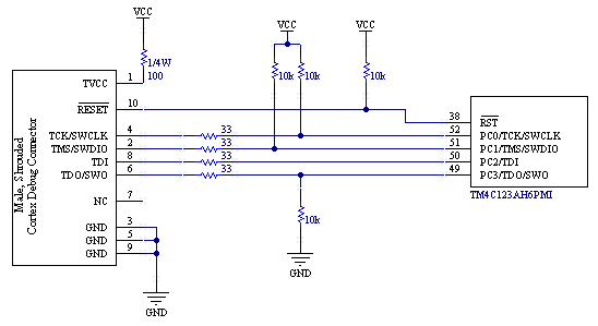
On our board, we have a 50mil connector with these connections:

1 - Pulled up to VCC through 100 ohm 1/4W resistor
2 - TMS/SWDIO
3 - GND
4 - TCK/SWCLK
5 - GND
6 - TDO/SWO
7 - Not connected
8 - TDI
9 - GND
10 - RESET

Program/debug works when using the built-in ICDI of a EK-TM4C123GXL LaunchPad with this custom board.


Target configuration:

<?xml version="1.0" encoding="UTF-8" standalone="no"?>
<configurations XML_version="1.2" id="configurations_0">
<configuration XML_version="1.2" id="Texas Instruments XDS110 USB Debug Probe_0">
        <instance XML_version="1.2" desc="Texas Instruments XDS110 USB Debug Probe_0" href="connections/TIXDS110_Connection.xml" id="Texas Instruments XDS110 USB Debug Probe_0" xml="TIXDS110_Connection.xml" xmlpath="connections"/>
        <connection XML_version="1.2" id="Texas Instruments XDS110 USB Debug Probe_0">
            <instance XML_version="1.2" href="drivers/tixds510cs_dap.xml" id="drivers" xml="tixds510cs_dap.xml" xmlpath="drivers"/>
            <instance XML_version="1.2" href="drivers/tixds510cortexM.xml" id="drivers" xml="tixds510cortexM.xml" xmlpath="drivers"/>
            <platform XML_version="1.2" id="platform_0">
                <instance XML_version="1.2" desc="Tiva TM4C123AH6PM_0" href="devices/tm4c123ah6pm.xml" id="Tiva TM4C123AH6PM_0" xml="tm4c123ah6pm.xml" xmlpath="devices"/>
            </platform>
        </connection>
    </configuration>
</configurations>

Elsewhere on this forum I read that someone solved the problem by rebooting. That did not help in our case.


  • While "feeling your pain" - it always proves interesting to note the, "need to DEBUG" - one's  (alleged),  "Debug Probe!"

    You've listed your, "ARM Standard, 10 pin (shrunk) JTAG/SWD connections" - yet is your "header orientation" - in full/proper accord w/that standard? Are external (i.e. proper) pull-up resistors present - upon the 4 JTAG lines? (internal Rs prove "risky" due to their >50K value)

    Use of that  "shrunken, 10 pin standard" has worked w/out issue for our firm - past 7-8 years (via J-Link) - w/out exception...

    Even having, "Been here/near "forever" - the error message you report - is beyond my recognition."       Surely your  Debug Tool provides a clear inventory listing of any/all such "Error Messages" - does it not?

  • This is what we have on the PCB:

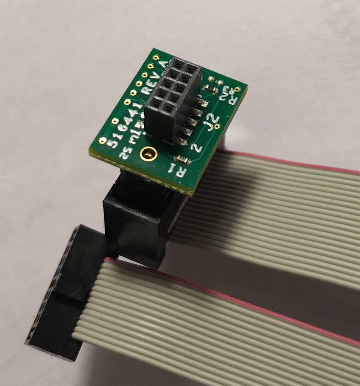
  •  It appears, though, that there are two 0402 package (1005 metric) resistors on the 10-pin adapter that came with the XDS110. Perhaps those are redundant to the ones on our board and should be removed? This is the adapter we used:

  • Is the schematic available for this 10-pin adapter? I could not find it in the XDS110 documentation or elsewhere.
  • This vendor (and/or predecessor) at one time produced a terrific adapter pcb, "ADA2-A" - which receives the standard 20 pin (0.1") ribbon cable and outputs via 10 pin (0.05") such cable.     In addition - a Reset Switch was thoughtfully included.      You (cannot) go wrong if you purchase this specific adapter - I suspect others supplied by this vendor may also succeed.      (yet we've not used)

    Firm/I employ only SWD - yet we note "TDI" (alone) w/out benefit of pull-up or pull-down.    (w/in your schematic)    That "inconsistency" demands - at minimum - your scope probing of this (uniquely treated signal) - to insure that it - transitions to spec.     (and is unburdened by reflections and/or less than square edges - usually resulting - from such "unaided" input.)

    As always - "Scope capture & save" of all JTAG Signals - from a "working board" - enables the effective "A-B" Comparison against your new (unfortunately issue impacted) board.

    Implementing such "A-B" comparison test  is the best means many believe (especially KISS followers)  -  to discover w/"high certainty  -  what  your JTAG issues truly are...

    You are "silent" as to the "meaning & value"  provided by vendor's  descriptive  error message.      Might you share the (assumed) detail such message  reports?

  • I thought the orientation was correct but it was not. With our board design, we have to plug in the probe so it looks backwards. Once you actually have it connected the right way, it works great :-)
  • Thank you for mentioning ADA2-A. I will look into that. Thanks as always for your help.
  • cb1_mobile said:
    10 pin (shrunk) JTAG/SWD connections" - yet is your "header orientation" - in full/proper accord w/that standard?

    Once again - even a "blind squirrel" may blunder (or stumble over) a  "walnut."     (I suspect the blood from my knee will slow (maybe stop) at some point...)      (maybe)

    Glad you persisted - more than once - MAJOR CLIENTS of ours have "mirror imaged" or otherwise (pardon) "butchered the header/connector!"     Experience proves a highly valued teacher - does it not?

    There's NEVER time to be detailed and careful ...  yet (always) time to "repair"  ...  pity ...  but does keep our  "back room behind a back room"  from  "going dark."

    (no squirrels  (blind or otherwise impaired) - nor  millennial staff  (often impaired) - were harmed during the creation of this posting.)      [same can not be said for crack "Remnant Carpet" ... "SO perfect"  for a "back-room"  - and now coated w/the "stumbled" cb1's blood] 

  • My blunders do tend to keep our rework guys busy as well. It's good job security! :-p

    I am sorry to hear that you have been hurt. Get well soon!