This thread has been locked.

If you have a related question, please click the "Ask a related question" button in the top right corner. The newly created question will be automatically linked to this question.

tm4c129encpdt: QSSI: Hold SSInFss low for continuous 24-bit transfer

Part Number: TM4C129ENCPDT
Other Parts Discussed in Thread: TM4C1294NCPDT,

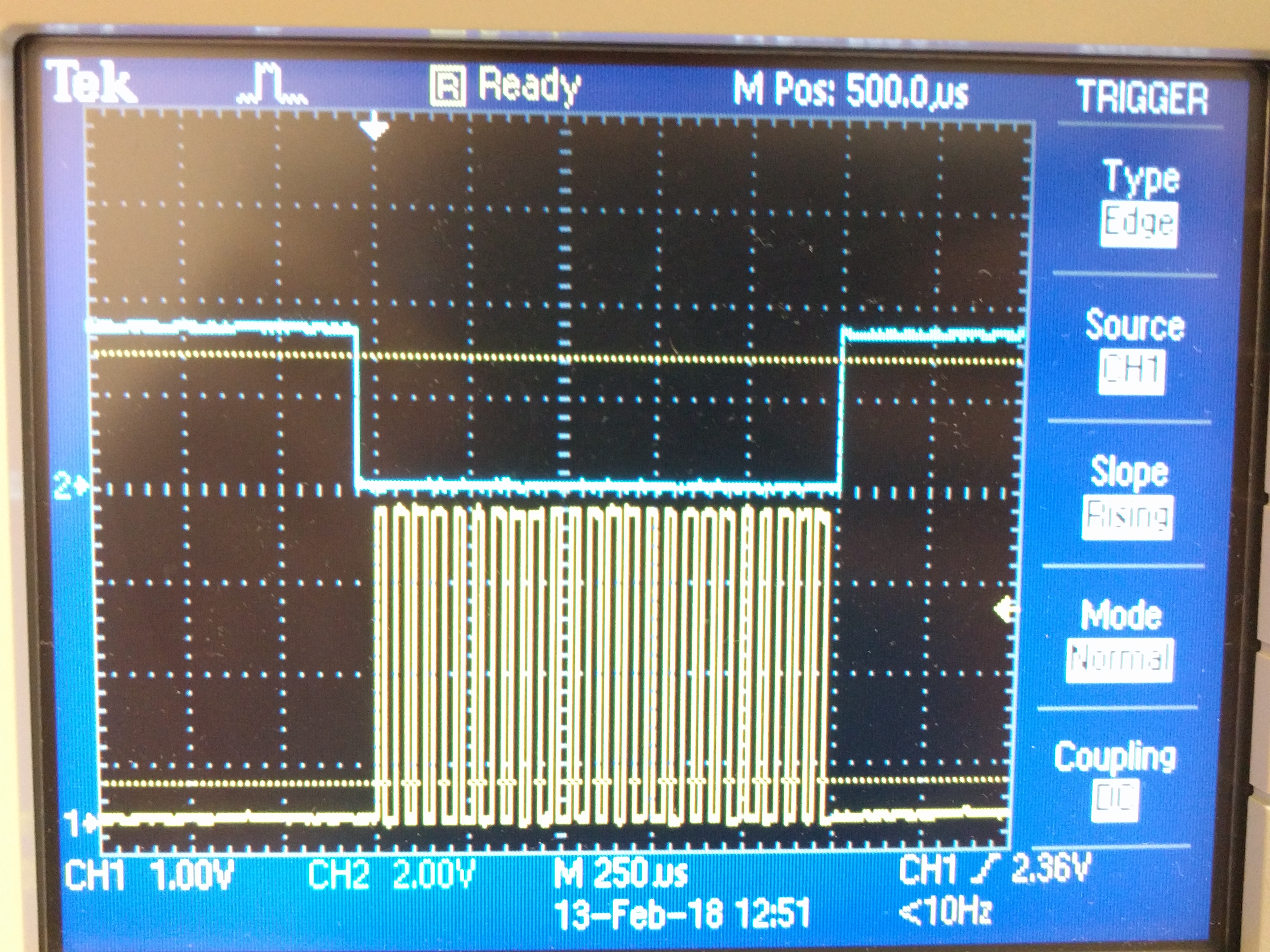
Using Freescale SPI format with SPO=0 and SPH=0, I need to transfer 24 bits and have SSInFss asserted low continuously for all 24 bits.

The datasheet seems to contain a contradiction.

Section 20.3.4 "SSInFSS Function" states:

"For Freescale format, with SPH = 0, the SSInFss signal is asserted low between continuous transfers. For SPH = 1, the SSInFss signal is deasserted (high) between continuous transfers."

But section 20.3.7.3 "Freescale SPI Frame Format with SPO=0 and SPH=0" states:

"However, in the case of continuous back-to-back transmissions, the SSInFss signal must be pulsed High between each data word transfer because the slave select pin freezes the data in its serial peripheral register and does not allow it to be altered if the SPH bit is clear. Therefore, the master device must raise the SSInFss pin of the slave device between each data transfer to enable the serial peripheral data write. On completion of the continuous transfer, the SSInFss pin is returned to its idle state one SSInClk period after the last bit has been captured."

Which is correct? How do we cause SSInFSS to remain low for the entire 24 bit transfer?

  • Agree w/your assessment of the (apparent) conflict w/in the MCU Manual. Tech-writer does appear  bit  "wobbly" in his/her description.

    I can report that several here "have succeeded" w/such 24 bit SPI transfers - yet if memory serves - in most "ALL" cases - the FSS function was controlled manually!    (i.e. the dedicated SPInFSS pin was NOT employed - instead a simple GPIO performed the FSS function.)

    Indeed this "Breaks from the (automatic) SPI transfer goal" - yet does, "Accomplish the SPI 24 bit transfer mission."      Your use of the Forum's Search Function, Keyword "16-24 bit SPI" - should produce several "hits."

    Might  "Quick/Dirty manual clarification" be gleaned by ordering up a 24 bit SPI transfer - and observing the behavior of the SPInFSS pin?     (while the SPI is config'ed for "automatic" FSSn mode...)

    I don't believe that  (either) "Quad or Bi" SPI transfers appeared w/in,  "Past forum search results."     (My sense is that a,  "24 bit SPI transfer" (as described here) most likely describes a "single-bit transfer" - not a "Bi or Quad" bit transfer...)

  • Hello

    Thank you for your input.

    I can toggle the SS line "manually" as a GPIO. It is annoying but not the end of the world that this eliminates the "fire-and-forget" SPI transfer I was hoping for.

    BUT...

    There appears to be a bigger problem. The part we're communicating with is a MAX11100 SPI ADC. It uses the SPI clock signal to time its acquisition and conversion process, as well as to shift out the resulting bits. From its datasheet, I bring you this statement: "Variations in frequency, duty cycle, or other aspects of the clock signal’s shape result in changing offset." So we need a really, really good clock. Unfortunately, looking at the clock signal on our oscilloscope, I can tell you that at the end of each 8-bit transfer, one clock pulse is stretched. That will result in unacceptable performance. I have to ensure that we get a nice proper clock for all 24 bits.

    Based on information from various posts in this forum, it seems that if there is additional data in the Tx FIFO after the end of a transmitted frame, the SSI peripheral should continue transmitting as a continuous back-to-back transfer; furthermore if code isn't stuffing the Tx FIFO fast enough and consequently one data word is shifted out completely before the next one appears in the Tx FIFO, that will lead to the transfer ending and then a new transfer beginning.

    We may be able to work around the SS issue by doing that manually, but we can't have the clock stretching. We looked for a way to disable the transmitter and stuff the Tx FIFO, then enable the transmitter, but it appears this peripheral does not support such operation. So we have decided to try with DMA and see if a burst transfer stuffs the Tx FIFO quickly enough.

    If that does not work... well, let's hope it works.
  • Ouch - the devil really lurks deeply in your newly provided specifics. As the Max chip vendor has "imposed such restriction" - one wonders, "How they advise hapless users?"

    You cannot be the "only one" bumping against this issue - that firm's FAE appears a most worthwhile destination.

    Might you clarify the use of "QSSI" which appeared w/in your Subject Line.    Is yours a "Bi or Quad" SPI transfer - my sense is no...

    Good luck - never have firm/I encountered so (strangely) demanding a device...

  • cb1_mobile said:

    Ouch - the devil really lurks deeply in your newly provided specifics. As the Max chip vendor has "imposed such restriction" - one wonders, "How they advise hapless users?"

    You cannot be the "only one" bumping against this issue - that firm's FAE appears a most worthwhile destination.

    Might you clarify the use of "QSSI" which appeared w/in your Subject Line.    Is yours a "Bi or Quad" SPI transfer - my sense is no...

    Good luck - never have firm/I encountered so (strangely) demanding a device...

    Perhaps I should have mentioned those details to begin with. But I didn't because I didn't want to muddy things up with a lot of extraneous details -- and at the time I didn't know that the clock stretching would occur on the 9th and 18th bits.

    To answer your question: We are using the SSI peripheral in Legacy Mode, Freescale SPI Mode, Master, without Advanced/Bi/Quad. The only reason I used QSSI in the subject line is to match up with the name given to this peripheral in the datasheet.

    Maybe we need to use Advanced mode, if we can get the correct waveform. I've read so many details in the datasheet that my head is spinning, but I seem to recall that we went with Legacy mode because Advanced will not provide the correct waveform for this purpose.

    And DMA is not helping. I was hoping (based on things I read elsewhere in the forum) that using DMA burst transfers to stuff the Tx FIFO more quickly than it can be un-stuffed by the peripheral might improve the situation. But take a look at the waveforms we're getting. These are with DMA -- however it looks exactly the same as without DMA:

    SSI3Fss:

    MORE IMPORTANTLY, this is what the all-important SSI3Clk  signal looks like:

    Notice those stretched 9th and 18th clocks. That will simply not do.

    As a good friend who could benefit from grammar lessons often says, "It don't work."

  • I continue in the belief that the "SPI chip vendor" is sure to be "more experienced" w/this issue - and is a likely asset.

    As you are being "plagued" (apparently) by the MCU's SPI (after-byte "re-grouping") - might simple, "bit-banging" enable a more consistent, "Data Clocking." (you would then have control over the data rate - and could likely (much reduce) any "stretched clocks.")

    One more Diagnostic item deserves consideration - are all scope-caps the result of, "Blind SPI Transmissions?"      You do not want (however unlikely) any "external factors" from "clouding" our analysis...    (while SPI is NOT I2C (where clock stretching often occurs) it is pointless to potentially enable any confounding, external disturbance...)

  • Hello twelve12pm,

    Yes it does appear the datasheet is poorly worded with regards to that section, I've taken a note of that inconsistency as I agree it is not well-written.

    Now then, regarding your issue, some questions to try and help...

    If you use a GPIO for the SS line instead, does the SPI clock still have a gap?
    How large is the gap?
    Whats your SPI clock speed vs your CPU speed?
    Have you tried loading all 24 bits into the FIFO before transmitting?
  • Hello Ralph,

    We like your logic in directing the, "Pre-Load all 24 bits prior to the SPI Transmission."     That said - iirc "Bob" suggested similarly (w/in another SPI post) and that "unwanted, extended clock pulse" still occurred - just as noted here...

    As "Bit-Banging" IS very "mechanical" - a method "Sure to Work" would employ, "24 bits worth of external, "Parallel-In - Serial Out" Shift Register."      Key here is the independent "load" of the 24 data bits - which would then be followed by a, "Highly consistent, MCU Timer's output" -  very well serving the (overly demanding) external device!      (which the MCU - thus far - has not!) 

    The Shift Registers would be placed in cascade - simplifying the design.     (Firm/I have done "just this" - via an FPGA - programmed to implement a 64 bit shifter.)

    While "blasphemy" (here) - the "Stand-Alone MCU" - does not always qualify as, "best method."      Sometimes the "Marriage of MCU & "purpose-based devices" - deliver the best (even the ONLY) solution...

  • Hi cb1,

    Yeah I am honestly suspecting that will still be the case, but depending on the tolerance for the extended pulse, I'm just fishing for ideas to help our friend should he want to avoid bit-banging. I had found another post from Amit who indicated that the size of the gap is partly due to the SPI vs System clock speed so that's where that question sprung from in addition to the others. Had got me thinking maybe that gap can be shrunk enough to be operable for the slave device.

    I certainly agree bit-banging would ultimately work though, and if there isn't a way to massage the peripheral to deliver the desired results, then that would need to be the solution of choice.
  • Hi Ralph,

    Thank you - we should note that "much of the appeal" garnered by "SPI" resulted from the presumed, "Ease & Robustness of Clocked Serial Data (both in & out)" - and that it was rare (almost never) that a, "Strict & Maintained frequency" - was forced upon the SPI clock!      The very purpose of that clock was to  "Escape" the devil, "timing demands" - required by Asynchronous Transfers...  (RS232/485 etc.)

    The external device vendor "Breaks both NEW & UNWANTED Ground" - in such a novel demand upon the MCU's (otherwise) hi-functioning SPI Peripheral Module.      (note too that cb1 is (sometimes) classed,  "hi/intermediate functioning" - but that only when, "pills are found/taken...")

  • Ralph, you've brought up a very interesting point: You asked if I tried loading all 24 bits into the FIFO before transmitting. I would like to do exactly that! The question is, how?
  • I saw a post by Amit suggesting that if there is additional data in the Tx FIFO when done transmitting a word, the next word is transmitted as part of a continuous transaction; if however the Tx FIFO is empty, the transaction is ended, SS goes high, etc., leading to the SS and CLK phenomena I show in my oscilloscope photos above. So, yes, I would like to pause the transmitter, stuff the Tx FIFO, and un-pause the transmitter -- and hopefully get the desired waveform! If you know how to do that, please enlighten me!
  • To answer Ralph's questions:

    System Clock is 120 MHz. SPI clock is 4 MHz.

    To solve the SS problem, we switched to using that pin as a GPIO rather than letting the peripheral control SS. The SPI clock still has the gaps every 8 bits. At 4 MHz the CLK cycle time should be 250 ns and the oscilloscope shows it is exactly that; however at the two gaps it is more like 1 uS.

    I thought that perhaps code wasn't loading the Tx FIFO quickly enough, so I implemented DMA to do it in a burst transfer. The output waveforms look exactly the same. No change. Since 24 bits (3 bytes) is less than a full burst transfer (4 bytes), I tried loading 4 bytes with DMA. That made no difference (except that now we're sending 32 bits, with all the same problems).

    Code:

    static uint8_t DummyByte = 0xff;
    static uint8_t Read[3];
    
    
    static inline void AssertChipSelect  (void) { MAP_GPIOPinWrite(GPIO_PORTF_BASE, GPIO_PIN_2, 0 ); }
    static inline void DeassertChipSelect(void) { MAP_GPIOPinWrite(GPIO_PORTF_BASE, GPIO_PIN_2, GPIO_PIN_2); }
    
    
    void InitMAX11100(void)
    {
    	uint32_t DummyRead;
    
    	// Set up port and pin for MAX11100 SPI chip select
    	MAP_GPIOPinTypeGPIOOutput(GPIO_PORTF_BASE, GPIO_PIN_2);
    	MAP_GPIOPadConfigSet(GPIO_PORTF_BASE, GPIO_PIN_2, GPIO_STRENGTH_4MA, GPIO_PIN_TYPE_STD);
    
    	// Startup SSI peripheral
    	MAP_SysCtlPeripheralDisable(SYSCTL_PERIPH_SSI3);
    	MAP_SysCtlPeripheralReset(SYSCTL_PERIPH_SSI3);
    	MAP_SysCtlPeripheralEnable(SYSCTL_PERIPH_SSI3);
    	while (MAP_SysCtlPeripheralReady(SYSCTL_PERIPH_SSI3) != true) {
    		// Wait for peripheral to activate
    	}
    
    	// Configure pin muxing for SSI
    	MAP_GPIOPinConfigure(GPIO_PF0_SSI3XDAT1);
    	//MAP_GPIOPinConfigure(GPIO_PF2_SSI3FSS);
    	MAP_GPIOPinConfigure(GPIO_PF3_SSI3CLK);
    
    	// Configure pins for use with SSI and give control to the SSI peripheral
    	MAP_GPIOPinTypeSSI(GPIO_PORTF_BASE, GPIO_PIN_0 /*| GPIO_PIN_2*/ | GPIO_PIN_3);
    
    	// Configure and enable SSI port for SPI master mode
    	MAP_SSIConfigSetExpClk(SSI3_BASE, Global.SysClockFreqHz, SSI_FRF_MOTO_MODE_0, SSI_MODE_MASTER, 4000000, 8);
    
    	// Enable the SSI module
    	MAP_SSIEnable(SSI3_BASE);
    
    	// Make sure Rx FIFO is empty before use
    	while (MAP_SSIDataGetNonBlocking(SSI3_BASE, &DummyRead)) {
    	}
    
    	// Connect appropriate DMA channels to the selected SSIs
    	MAP_uDMAChannelAssign(UDMA_CH14_SSI3RX);
    	MAP_uDMAChannelAssign(UDMA_CH15_SSI3TX);
    
    	// Make sure unneeded Rx channel DMA attributes are off
    	MAP_uDMAChannelAttributeDisable(UDMA_CH14_SSI3RX, UDMA_ATTR_ALTSELECT | UDMA_ATTR_USEBURST | UDMA_ATTR_HIGH_PRIORITY | UDMA_ATTR_REQMASK);
    
    	// Set Rx DMA primary control structure:
    	// - Data size 8 bits
    	// - Source address does not increment; always points to SSI Rx data register
    	// - Destination address increment is 8-bit
    	// - Arbitration size is 4 to match SSI Rx FIFO trigger threshold
    	// - DMA will use 4 frame burst transfer if possible for efficiency
    	MAP_uDMAChannelControlSet(
    		UDMA_CH14_SSI3RX | UDMA_PRI_SELECT,
    		UDMA_SIZE_8 | UDMA_SRC_INC_NONE | UDMA_DST_INC_8 | UDMA_ARB_4
    	);
    
    	// Make sure unneeded Tx channel DMA attributes are off
    	MAP_uDMAChannelAttributeDisable(UDMA_CH15_SSI3TX, UDMA_ATTR_ALTSELECT | UDMA_ATTR_HIGH_PRIORITY | UDMA_ATTR_REQMASK);
    
    	// Enable USEBURST to force Tx channel DMA to always use burst when
    	// transferring from Tx buffer to SSI.
    	MAP_uDMAChannelAttributeEnable(UDMA_CH15_SSI3TX, UDMA_ATTR_USEBURST);
    
    	// Set Tx DMA primary control structure:
    	// - Data size 8 bits
    	// - Source address does not increment; we always send same dummy data
    	// - Destination address does not increment; always points to SSI Tx data register
    	// - Arbitration size is 4 to match SSI Tx FIFO trigger threshold
    	MAP_uDMAChannelControlSet(
    		UDMA_CH15_SSI3TX | UDMA_PRI_SELECT,
    		UDMA_SIZE_8 | UDMA_SRC_INC_NONE | UDMA_DST_INC_NONE | UDMA_ARB_4
    	);
    }
    
    
    uint32_t ReadMAX11100(void)
    {
    	AssertChipSelect();
    
    	// Set up DMA to read 3 bytes
    	// ==========================
    
    	// Set Rx DMA primary control structure transfer parameters:
    	// - Mode set to basic (not ping-pong).
    	// - Source is SSI data register
    	// - Destination is receive memory buffer
    	// - Transfer size is set to match the size of the buffer
    	//
    	MAP_uDMAChannelTransferSet(
    		UDMA_CH14_SSI3RX | UDMA_PRI_SELECT,
    		UDMA_MODE_BASIC,
    		(void *)(SSI3_BASE + SSI_O_DR),
    		(void *) Read,
    		3
    	);
    
    	// Enable channel because it is disabled at completion of each transfer
    	MAP_uDMAChannelEnable(UDMA_CH14_SSI3RX);
    
    	// Enable DMA on SSI side
    	MAP_SSIDMAEnable(SSI3_BASE, SSI_DMA_RX);
    
    
    	// Set up DMA to write 3 bytes
    	// ===========================
    
    	// Set Tx DMA primary control structure transfer parameters:
    	// - Mode must be set to basic (not ping-pong) because peripheral is making the request.
    	// - Source transmit memory buffer
    	// - Destination is SSI data register
    	// - Transfer size is set to size of buffer
    	MAP_uDMAChannelTransferSet(
    		UDMA_CH15_SSI3TX | UDMA_PRI_SELECT,
    		UDMA_MODE_BASIC,
    		(void *) &DummyByte,
    		(void *)(SSI3_BASE + SSI_O_DR),
    		3
    	);
    
    	// Enable channel because it is disabled at completion of each transfer
    	MAP_uDMAChannelEnable(UDMA_CH15_SSI3TX);
    
    	// Enable DMA on SSI side
    	// Tell SSI peripheral to enable DMA
    	MAP_SSIDMAEnable(SSI3_BASE, SSI_DMA_TX);
    
    
    	// Wait for DMA to complete
    	// ========================
    
    	while (MAP_uDMAChannelModeGet(UDMA_CH14_SSI3RX | UDMA_PRI_SELECT) != UDMA_MODE_STOP) {
    	}
    
    	DeassertChipSelect();
    
    	return ((Read[1] & 0xff) << 8) | (Read[2] & 0xff);
    }
    

    Suggestions?

  • To answer cb1's question about bit-banging the SPI transfer: I really hope to avoid doing that. I've been able to work with parts like the MAX11100 from other MCUs which shall remain nameless, but which can do 32 bit SPI transfers. Everything I've read and understood (if I understood anything at all) from the datasheet tells me that I should be able to get the nice consistent waveform that I need... The question is, what about my setup is preventing that from working successfully?
  • twelve12pm said:
    The question is, what about my setup is preventing that from working successfully?

    I'm "Not so sure" that you've identified the correct question!"       Have not (others) here - reported that same "irregularity" (Ans: they HAVE!) - it is thus unlikely that they employed,  "your setup!"      Or that you have "caused" such issue!

    twelve12pm said:
    the datasheet tells me that I should be able to get the nice consistent waveform that I need...

    Where do you see that?    (we do NOT ... Is it not "most likely" that you are viewing an "easily drawn/produced" repetitive clocking - and not one which "staggers" @ byte intervals?)

    As I wrote (to silence) the "Clocked Data" of SPI was intended to prove more robust than (older) asynchronous methods.     I cannot recall that (any) tight consistency was, "forced upon the SPI clock" (other than normal/customary "set-up/hold times."     You appear to have NOT challenged the external device vendor - surely THEY encounter such (fairly raised) issue FAR MORE than do those - here!

    Like you - my firm employs (other) ARM MCUs - and we have noted that (some) produce the "regular output clock you seek" - while others - do not!      (How wonderful!)

    Seeking to "escape" such limitation (w/in that peripheral & others) - my firm has migrated such functions to a, "Selectively filled" device on our pcb (an FPGA) which provides a most helpful,  "Performance Generalization - enhancing the use of various ARM MCUs" - which "Speeds, Eases & Enhances" VALUE DELIVERY to our clients...      

    Deciding to attempt to, "Tease Out" - such "normally expected behavior" (from a "resistant device" (here)) - is "one route" - but we doubt that proves, "best route..."     (and the Delivery clock IS ticking...)

  • Hello twelve12pm,

    Well, I may have stuck my foot in my mouth a bit RE: loading the FIFO beforehand. I've tried a variety of measures even as far as DRM's (which we are supposed to avoid with TivaWare being available!) and haven't had any luck getting rid of the pesky period between bytes.

    I was only able to somewhat 'succeed' (I say that *extremely* loosely) by trying something which I afterwards found out violates not only the DS specs but it should have made TivaWare scream errors at me as well... why the MCU didn't freak out but actually do what I had incorrectly asked of it is unclear, though the fact that it didn't go off the deep end has me pondering if there somehow is some sort of workaround. I'll dig deeper tomorrow to try and follow that faint sliver of light, but I'll forewarn that I am highly hesitant there is anything truly workable there.

    For the moment, I think the issue is the limiting factor imposed by Register QSSI Control 0 which sets the maximum allowed QSSI Data Size to be 0xF - i.e 16 bits.
  • Ralph Jacobi said:
    Hello twelve12pm,

    Well, I may have stuck my foot in my mouth a bit RE: loading the FIFO beforehand. I've tried a variety of measures even as far as DRM's (which we are supposed to avoid with TivaWare being available!) and haven't had any luck getting rid of the pesky period between bytes.

    I was only able to somewhat 'succeed' (I say that *extremely* loosely) by trying something which I afterwards found out violates not only the DS specs but it should have made TivaWare scream errors at me as well... why the MCU didn't freak out but actually do what I had incorrectly asked of it is unclear, though the fact that it didn't go off the deep end has me pondering if there somehow is some sort of workaround. I'll dig deeper tomorrow to try and follow that faint sliver of light, but I'll forewarn that I am highly hesitant there is anything truly workable there.

    For the moment, I think the issue is the limiting factor imposed by Register QSSI Control 0 which sets the maximum allowed QSSI Data Size to be 0xF - i.e 16 bits.

    I appreciate greatly your help on this matter.

    I will be intrigued to hear what out-of-spec thing you've discovered.

  • cb1_mobile said:

    As I wrote (to silence) the "Clocked Data" of SPI was intended to prove more robust than (older) asynchronous methods.     I cannot recall that (any) tight consistency was, "forced upon the SPI clock" (other than normal/customary "set-up/hold times."     You appear to have NOT challenged the external device vendor - surely THEY encounter such (fairly raised) issue FAR MORE than do those - here!

    Apologies for said silence. That was unintentional. I'll let you know what I find out...

  • Again - is it not quite clear that the "perpetrator" of the (overly demanding, "dead-consistent," SPI clock march) is "Sure to have heard this issue/complaint" - far more often than the crüe here?

    Ralph has made a significant effort - yet if he must resort to "bending the rules" - there is NO/ZERO guarantee that (any) future process tweak - will enable that "magic" to continue!      What then?      (House of cards - anyone?)    

    Periodically we are engaged by VCs - they direct us to, "search for such rule bendings" - and reject those who, "game the system..."     (Risk registers as, "Way too high!")

  • cb1_mobile said:

    Again - is it not quite clear that the "perpetrator" of the (overly demanding, "dead-consistent," SPI clock march) is "Sure to have heard this issue/complaint" - far more often than the crüe here?

    Ralph has made a significant effort - yet if he must resort to "bending the rules" - there is NO/ZERO guarantee that (any) future process tweak - will enable that "magic" to continue!      What then?      (House of cards - anyone?)    

    Periodically we are engaged by VCs - they direct us to, "search for such rule bendings" - and reject those who, "game the system..."     (Risk registers as, "Way too high!")

    Yes. We contacted the "perpetrator" yesterday and are awaiting reply. Hopefully someone knowledgeable from their "motley crüe" will be in contact shortly. I will let you know what we learn.
  • Staff/I "aspire" to such "motley-ness." (that's a good catch - 12squared...)
    I would suggest that you make "good note" of the "unusual requirement" - forced upon TM4C's hapless SPI clock mechanism - by Maxi's crüe ...
  • I managed to hold the FSS signal low for an entire 24 bit frame on a TM4C129XN. Your risk is the note on SSIAdvFrameHoldEnable() "The availability of the advanced mode of SSI operation varies with the Tiva part and SSI in use. Please consult the data sheet for the part in use to determine whether this support is available"

    I don't know what to check in the datasheet. You can try my code. If it works it works!

    /*
     * main.c
     */
    
    #include <stdint.h>
    #include <stdbool.h>
    
    //propabaly dont need most of these includes
    #include <inc/hw_ints.h>
    #include <inc/hw_memmap.h>
    #include <inc/hw_types.h>
    #include <inc/hw_gpio.h>
    
    #include <driverlib/flash.h>
    #include <driverlib/gpio.h>
    #include <driverlib/i2c.h>
    #include <driverlib/pin_map.h>
    #include <driverlib/pwm.h>
    #include <driverlib/ssi.h>
    #include <driverlib/sysctl.h>
    #include <driverlib/uart.h>
    #include <driverlib/udma.h>
    #include <driverlib/lcd.h>
    #include <driverlib/epi.h>
    #include <driverlib/interrupt.h>
    
    
    #include "inc/hw_gpio.h"
    #include "inc/hw_ints.h"
    #include "inc/hw_memmap.h"
    #include "inc/hw_sysctl.h"
    #include "inc/hw_types.h"
    #include "driverlib/debug.h"
    #include "driverlib/gpio.h"
    #include "driverlib/interrupt.h"
    #include "driverlib/ssi.h"
    
    int main(void) {
    
        //set a 25MHz system clock
        uint32_t sysClk = SysCtlClockFreqSet((SYSCTL_XTAL_25MHZ | SYSCTL_OSC_MAIN | SYSCTL_USE_PLL | SYSCTL_CFG_VCO_480), 25000000);
    
        SysCtlPeripheralEnable(SYSCTL_PERIPH_SSI1);
        SysCtlPeripheralEnable(SYSCTL_PERIPH_GPIOB);
        SysCtlPeripheralEnable(SYSCTL_PERIPH_GPIOE);
        while(!SysCtlPeripheralReady(SYSCTL_PERIPH_SSI1));
        while(!SysCtlPeripheralReady(SYSCTL_PERIPH_GPIOB));
        while(!SysCtlPeripheralReady(SYSCTL_PERIPH_GPIOE));
    
    
        GPIOPinConfigure(GPIO_PB4_SSI1FSS);
        GPIOPinTypeSSI(GPIO_PORTB_BASE , GPIO_PIN_4);
        GPIOPinConfigure(GPIO_PB5_SSI1CLK);
        GPIOPinTypeSSI(GPIO_PORTB_BASE , GPIO_PIN_5);
        GPIOPinConfigure(GPIO_PE4_SSI1XDAT0);
        GPIOPinTypeSSI(GPIO_PORTE_BASE , GPIO_PIN_4);
    
    
        SSIConfigSetExpClk(SSI1_BASE, sysClk, SSI_FRF_MOTO_MODE_0, SSI_MODE_MASTER, 19200, 8);
    
        SSIAdvFrameHoldEnable(SSI1_BASE);
        SSIAdvModeSet(SSI1_BASE, SSI_ADV_MODE_WRITE);
    
        //interface must be configured before it is enabled
        SSIEnable(SSI1_BASE);
    
        //delay loop to show FSS high on scope
        int i;
        for(i = 0; i <500000; i++);
    
        SSIDataPut(SSI1_BASE, 0xff);
        SSIDataPut(SSI1_BASE, 0x55);
        SSIAdvDataPutFrameEnd(SSI1_BASE, 0x64);
    
        while(1);
    }
    

  • Your scope-cap would prove, "Far more useful" if it revealed the (expected) SPI clock's "deviation" (or not) - noted at "byte intervals" - and which proves destructive to "12-12's" unique quest...

    The issue was "not" with "FSS" - it was the SPI clock's deviation - as (above) stated...
  • Hey Peter,

    Nice find!! The datasheet didn't describe anything in Advanced mode for SSI that made me think it would be useful for this, had no idea it was capable of that. Advanced SSI is mentioned in the datasheet for the device twelve12pm is using by the way.

    I went ahead and confirmed that your method will work for the TM4C1294NCPDT as well, so that looks to be the solution for the issue.

    And cb1, measured with my LSA and the clocks are perfectly distributed for me, no gap at all between any bytes, and the SS line behaves without needing to assign it to a GPIO as well. The scope is shows no lies.
  • The TivaWare API has spoiled me. Sometimes its tempting to not check the datasheet at all...
  • Woohoo!

    Dear Peter,

    Thank you very much for this! I tested and the clock gaps are indeed removed.

    Perhaps I should just ignore the datasheet from now on and just go with TivaWare calls :-)

    Here is what I did: I basically added these two calls to my code, just before the call to SSIEnable():

    	MAP_SSIAdvFrameHoldEnable(SSI3_BASE);
    	MAP_SSIAdvModeSet(SSI3_BASE, SSI_ADV_MODE_READ_WRITE);
    

    That removed the gaps in my SPI clock waveform!

    There are some caveats though.

    I am still controlling the SSI3FSS pin manually, as a GPIO.

    Here's why:

    We have a quite a few interrupts in the system. If I make calls like these:

    SSIDataPut(SSI1_BASE, 0xff);
    SSIDataPut(SSI1_BASE, 0x55);
    SSIAdvDataPutFrameEnd(SSI1_BASE, 0x64);
    

    Then there is a good possibility of an interrupt happening between them, which would lead to the Tx FIFO becoming depleted before all data is in place, which would subsequently cause a (relatively) very long clock gap. I did not see a way to "pause the transmitter" so I could stuff the Tx FIFO at leisure and then start transmitting when ready. (If there is a way to do this, please enlighten me!)

    I can of course pause interrupts with IntMasterDisable() and IntMasterEnable(), but I avoid that like the plague.

    So, since I had already implemented the code to stuff the SSI Tx FIFO using DMA as described in prior posts, I kept that code as-is, added the calls to SSIAdvFrameHoldEnable() and SSIAdvModeSet() and observed their effect on the clock signal:

    Namely, no more gaps!

    The gaps from before were about 4 clock periods in length, so they were clearly visible.

    BUT! There is a caveat with the DMA:

    I do not see any way to place a 1 in the SSI's CR1.EOM bit to indicate Stop Frame, when using DMA. The DMA is only able to stuff one peripheral register repeatedly, that being the data register (Tx FIFO). As I see it, EOM is in a different register and must be set BEFORE the last byte is placed, so I can't wait for a DMA completion interrupt to do so.

    That does not appear to have any effect on the SPI clock waveform. But it does affect SSI3FSS in that as far as the SSI peripheral is concerned, the frame never ends, so it never deasserts SSI3FSS.

    In the datasheet (uh oh, I'm looking at it again!) the EOM description is: "This bit is applicable when MODE is set to Advanced, Bi- or Quad- SSI. This bit is inserted into bit 12 of the TXFIFO data entry by the QSSI module."

    I thought, hmmmm, what if I set the DMA to 16 bit transfers instead of 8 bit, and stuff 0x00ff, 0x00ff, 0x10ff into the Tx FIFO? But sadly, that did not work. I think those upper 8 bits are somehow masked out when using Advanced mode, which forces 8-bit transfers. So, unless someone enlightens me as to another cool trick, I continue to control the chip select line as a GPIO.

    With the clock gaps removed, I'm happy as a pig eating slop.

    Thanks to everyone for your generous help: cb1, Ralph, and Peter.

    Code:

    void InitMAX11100(void)
    {
    	uint32_t DummyRead;
    
    	// Set up port and pin for SPI chip select
    	MAP_GPIOPinTypeGPIOOutput(GPIO_PORTF_BASE, GPIO_PIN_2);
    	MAP_GPIOPadConfigSet(GPIO_PORTF_BASE, GPIO_PIN_2, GPIO_STRENGTH_4MA, GPIO_PIN_TYPE_STD);
    
    	MAP_SysCtlPeripheralDisable(SYSCTL_PERIPH_SSI3);
    	MAP_SysCtlPeripheralReset(SYSCTL_PERIPH_SSI3);
    	MAP_SysCtlPeripheralEnable(SYSCTL_PERIPH_SSI3);
    	while (MAP_SysCtlPeripheralReady(SYSCTL_PERIPH_SSI3) != true) {
    		// Wait for peripheral to activate
    	}
    
    	// Configure pin muxing for SSI
    	MAP_GPIOPinConfigure(GPIO_PF0_SSI3XDAT1);
    	MAP_GPIOPinConfigure(GPIO_PF3_SSI3CLK);
    
    	// Configure pins for use with SSI and give control to the SSI peripheral
    	MAP_GPIOPinTypeSSI(GPIO_PORTF_BASE, GPIO_PIN_0 | GPIO_PIN_3);
    
    	// Configure and enable SSI port for SPI master mode
    	MAP_SSIConfigSetExpClk(SSI3_BASE, Global.SysClockFreqHz, SSI_FRF_MOTO_MODE_0, SSI_MODE_MASTER, 4000000, 8);
    
    	// Enable advanced mode to allow transmitting continuously for three bytes
    	// without clock gaps.
    	//
    	// Caveats:
    	// 1. Because we are using DMA, it seems we cannot load the EOM (End Of
    	//    Message) bit of the SSI's CR1 register. That means that chip select
    	//    will never be deasserted. Therefore we must control chip select as
    	//    a GPIO.
    	// 2. This will only work when SPI mode is SSI_FRF_MOTO_MODE_0!! This is
    	//    the case for MAX11100 but may be different for other SPI ICs.
    	MAP_SSIAdvFrameHoldEnable(SSI3_BASE);
    	MAP_SSIAdvModeSet(SSI3_BASE, SSI_ADV_MODE_READ_WRITE);
    
    	// Enable the SSI module
    	MAP_SSIEnable(SSI3_BASE);
    
    	// Make sure Rx FIFO is empty before use
    	while (MAP_SSIDataGetNonBlocking(SSI3_BASE, &DummyRead)) {
    	}
    
    	// Connect appropriate DMA channels to the selected SSIs
    	MAP_uDMAChannelAssign(UDMA_CH14_SSI3RX);
    	MAP_uDMAChannelAssign(UDMA_CH15_SSI3TX);
    
    	// Make sure unneeded Rx channel DMA attributes are off
    	MAP_uDMAChannelAttributeDisable(UDMA_CH14_SSI3RX, UDMA_ATTR_ALTSELECT | UDMA_ATTR_USEBURST | UDMA_ATTR_HIGH_PRIORITY | UDMA_ATTR_REQMASK);
    
    	// Set Rx DMA primary control structure
    	MAP_uDMAChannelControlSet(
    		UDMA_CH14_SSI3RX | UDMA_PRI_SELECT,
    		UDMA_SIZE_8 | UDMA_SRC_INC_NONE | UDMA_DST_INC_8 | UDMA_ARB_4
    	);
    
    	// Make sure unneeded Tx channel DMA attributes are off
    	MAP_uDMAChannelAttributeDisable(UDMA_CH15_SSI3TX, UDMA_ATTR_ALTSELECT | UDMA_ATTR_HIGH_PRIORITY | UDMA_ATTR_REQMASK);
    
    	// Enable USEBURST to force Tx channel DMA to always use burst when
    	// transferring from Tx buffer to SSI.
    	MAP_uDMAChannelAttributeEnable(UDMA_CH15_SSI3TX, UDMA_ATTR_USEBURST);
    
    	// Set Tx DMA primary control structure
    	MAP_uDMAChannelControlSet(
    		UDMA_CH15_SSI3TX | UDMA_PRI_SELECT,
    		UDMA_SIZE_8 | UDMA_SRC_INC_NONE | UDMA_DST_INC_NONE | UDMA_ARB_4
    	);
    }
    
    
    uint32_t ReadMAX11100(void)
    {
    	static uint8_t DummyByte = 0xff;
    	static uint8_t Read[3];
    
    	// Assert chip select
    	MAP_GPIOPinWrite(GPIO_PORTF_BASE, GPIO_PIN_2, 0); 
    
    	// Set up DMA to read 3 bytes
    	MAP_uDMAChannelTransferSet(
    		UDMA_CH14_SSI3RX | UDMA_PRI_SELECT,
    		UDMA_MODE_BASIC,
    		(void *)(SSI3_BASE + SSI_O_DR),
    		(void *) Read,
    		3
    	);
    
    	// Enable channel because it is disabled at completion of each transfer
    	MAP_uDMAChannelEnable(UDMA_CH14_SSI3RX);
    
    	// Enable DMA on SSI side
    	MAP_SSIDMAEnable(SSI3_BASE, SSI_DMA_RX);
    
    	// Set up DMA to write 3 bytes
    	MAP_uDMAChannelTransferSet(
    		UDMA_CH15_SSI3TX | UDMA_PRI_SELECT,
    		UDMA_MODE_BASIC,
    		(void *) &DummyByte,
    		(void *)(SSI3_BASE + SSI_O_DR),
    		3
    	);
    
    	// Enable channel because it is disabled at completion of each transfer
    	MAP_uDMAChannelEnable(UDMA_CH15_SSI3TX);
    
    	// Enable DMA on SSI side
    	MAP_SSIDMAEnable(SSI3_BASE, SSI_DMA_TX);
    
    	// Wait for DMA to complete
    	while (MAP_uDMAChannelModeGet(UDMA_CH14_SSI3RX | UDMA_PRI_SELECT) != UDMA_MODE_STOP) {
    	}
    
    	// Deassert chip select
    	MAP_GPIOPinWrite(GPIO_PORTF_BASE, GPIO_PIN_2, GPIO_PIN_2); 
    
    	return ((Read[1] & 0xff) << 8) | (Read[2] & 0xff);
    }


    This is on TM4C129ENCPDT.

  • cb1_mobile said:
    Staff/I "aspire" to such "motley-ness." (that's a good catch - 12squared...)
    I would suggest that you make "good note" of the "unusual requirement" - forced upon TM4C's hapless SPI clock mechanism - by Maxi's crüe ...

    I like the name 12squared! Maybe I should call myself 12cubed :-)

  • Kudos to poster Peter,  to Ralph, and (especially) to "12-12" for the (really) terrific narratives - and scope caps - and the valuable descriptions of, "How you proceeded based upon "facts at hand."

    Due to Peter's scope cap (compressing) the data clocks - I feared that he may have missed the central issue.       And - he VERY MUCH - did NOT!    Bravo, Peter.     (kicked my opinionated rear...)

    I believe that it (still) proves of value to request that vendor's Ralph contact the group charged w/the MCU's SPI implementation - it would prove of interest to learn:

    • was the (somewhat) unexpected "broadening" of the SPI clock - noted at repeated "byte intervals" -  "a deliberate part of their intended SPI implementation mechanism?"
    • and - based upon that response - is this "fix" likely (guaranteed, even stronger) to "hold" - even when - especially when - new chip revisions and/or process tweaks arrive?

    As both 12-12 and my group have noted (being users of multiple vendors' ARM MCUs) certain other MCUs exhibit this clock deviation - while others - do not!     (how delightful)

    While "all (appears) well" (for now) - we've had first-hand experience where such "special modes" (may) exhibit "shifted behavior" - due to chip revisions and/or (inevitable) process tweaks.    Uh-Oh!

    To (one last time...Ha!) beat the "dead horse" - it would still prove of interest to learn, "Guidance provided by the external chip vendor - enforcing this (unwanted) SPI clock restriction..."

    And kudos to 12-12 for, "Fitting exactly 24 SPI clocks - and FILLING the scope's width (even "Little Stevie Wonder" could view) - in so doing!      Great attention to detail - and you (even) thanked your (but for Peter) hapless crüe...   (only one crüe member"solved" this puzzle - although our FPGA method surely would have worked - and is MCU Agnostic!    Required if/when you, "Chase BIG Bucks!")

  • Hello twelve12pm,

    The key isn't so much as halting the transmit for when the FIFO is full as it is both doing that and making SS behave... I can load up bytes with nice delays to simulate interrupts getting in the way into the FIFO and they'll sit without TX until I send SSIEnable, but during that time the SS line decides it wants to be low already. Not terribly surprising given the SSIEnable/Disable API's aren't supposed to be used that way I suppose, but it does make that method not work. There doesn't seem to be an alternate method to preloading the FIFO.

    As far as the DMA goes, I am not currently seeing a way to get the DMA to do what would be required to get away from the manual SS either.

    The key for the Stop Frame being executed right is not loading bit 12 into the TX FIFO, but it's setting the register flag for End of Message:

    HWREG(ui32Base + SSI_O_CR1) |= SSI_CR1_EOM;

    That is what the FrameEnd functions are doing to ensure the SS line goes high. I searched driverlib and found no trace of the SSI_CR1_EOM variable being used outside the two advanced mode frame end SSI functions though.

    The only way you could maybe work around it would be to not just use a direct register call, but find out how to add that so that it is only set when the uDMA has 1 byte left to send out... I don't think that'd be worthwhile to chase after over the current solution given the complexity. I think we've reached the limit of the TM4C's kitchen sink abilities.

  • Hello cb1,

    Request heard loud and clear, but unfortunately may be hard to follow through on. Not sure who all owned that portion, but as the device has been around for a long time and designed long ago... might be hard to get info straight from the horses mouth who handled that exact implementation. Though I did take down plenty of notes from this whole thread for our own internal reference.

    For what it's worth, from all my digging into this though, I would say both aspects are working as intended. The Advanced mode features are geared towards adding additional functionality that is not offered by the standard SSI module implementation. That includes giving an explicit setting that forces the SS line low, which the SSI module does not have. Based on that, it isn't unreasonable to assume that the SSI module in it's standard implementation was designed to have SS pulse between each byte, so thus even though SS is removed from it's control, the logic of the state machine still waits for that pulse before loading the next byte.

    If I am right about all of that, then both modes should continue to work in all devices with Advanced SSI that supports the Frame End feature, as it seems that feature was very intentionally designed into the device to cover cases where the SS pulse is not beneficial such as in twelve12pm's case.

  • Hello twelve12pm,

    One more thing I'd be remiss to not mention!! Since we are now talking about Advanced mode for SSI... please take care to avoid running head first into Errata SSI#03 (http://www.ti.com/lit/er/spmz850g/spmz850g.pdf) :)

    Note: Peter seems to be a wizard as his device should be affected too...

  • AAaaahhhh!!!

    Luckily this particular SSI channel is on SSI3, which is unaffected by that erratum.

    However I *just* started working on the next SSI task, which is using SSI1. Hopefully we will not need Advanced mode for that.

    Thank you for the reminder.
  • cb1_mobile said:

    And kudos to 12-12 for, "Fitting exactly 24 SPI clocks - and FILLING the scope's width (even "Little Stevie Wonder" could view) - in so doing!      Great attention to detail - and you (even) thanked your (but for Peter) hapless crüe...   (only one crüe member"solved" this puzzle - although our FPGA method surely would have worked - and is MCU Agnostic!    Required if/when you, "Chase BIG Bucks!")

    I'm glad you liked that!

    A few years ago I spent quite some time learning FPGAs and CPLDs for a project we ended up doing another way but I'm sure there will be FPGAs in our eventual future.

  • Hello Ralph,

    Thank you - once again - you've gone, "FAR Beyond" that requested.

    And indeed - TM4C (is) "showing its age."     And (some) here may sense that (sometime)... maybe ... "New Devices (may appear) on the horizon!"      

    Would it not prove "useful" to, "Relay this thread" so that the, (pardon) "Sins of the past" do not, "Invade the new devices'  future?"      (Poster Peter may not (still) be available for a "repeat" rescue...)

  • cb1_mobile said:

    And indeed - TM4C (is) "showing its age."     And (some) here may sense that (sometime)... maybe ... "New Devices (may appear) on the horizon!"      

    Would it not prove "useful" to, "Relay this thread" so that the, (pardon) "Sins of the past" do not, "Invade the new devices'  future?"      (Poster Peter may not (still) be available for a "repeat" rescue...)

    PLEASE don't give them any ideas about age! Or, as a corollary, about (Lord forbid) obsoleting this family.
    For perfectly valid reasons, technical and otherwise, we've selected the TM4C family for our new products. This represents a costly migration from another vendor and completely different MCU family, and requires basically a rewrite of our software, which is quite sizable, has taken months already, and isn't finished yet. Yes, we have high level processor independent code which is separate from the low level nuts and bolts code, but this being an embedded system with hard real-time requirements, you can't avoid having a large amount of low level code that is tied very strongly to the MCU and that must work exactly right. Take this clock gap issue for example. If we switch MCU families, we have to solve that (and a thousand other things) all over again. Needless to say, we've made a tremendous commitment to TM4C and a significant investment in cost, time, effort, etc.
    Every MCU from every vendor comes with its idiosyncrasies and shortcomings and while TM4C comes with a few surprises of its own, so far it appears to be doing a great job. I'm confident we've chosen the best MCU family to fit our new products.
    Having said all of that, if there are new MCUs in the making, I do have a (long) wish list :-)
    Just don't obsolete this one!
  • Hi cb1,

    cb1_mobile said:
    Would it not prove "useful" to, "Relay this thread" so that the, (pardon) "Sins of the past" do not, "Invade the new devices'  future?"

    Hence my comment of:

    Ralph Jacobi said:
    Though I did take down plenty of notes from this whole thread for our own internal reference.

    Also twelve12pm, no need to worry, TM4C isn't going anywhere!! You'll be happy with the design choice I'm sure :)

  • Somehow, "Taking such notes for internal reference" is not as "active" as, "Relaying the entire thread" - which "insures" that the design group receives the "full & complete flavor" - of this (very) active thread.

    As a past member of  "such a design team" - we most always sought the, "Full & unfiltered story" (along w/individual notes) - and it was that,  "combination... weighed together" - which proved most beneficial & instructive...     (notes (alone) cannot provide the thread's "ebb & flow" - nor report the datasheet's "strength & weaknesses" (as was SO well detailed here) and are subject/vulnerable to,  "personal interpretation.")