A related question is a question created from another question. When the related question is created, it will be automatically linked to the original question.
If you have a related question, please click the "Ask a related question" button in the top right corner. The newly created question will be automatically linked to this question.
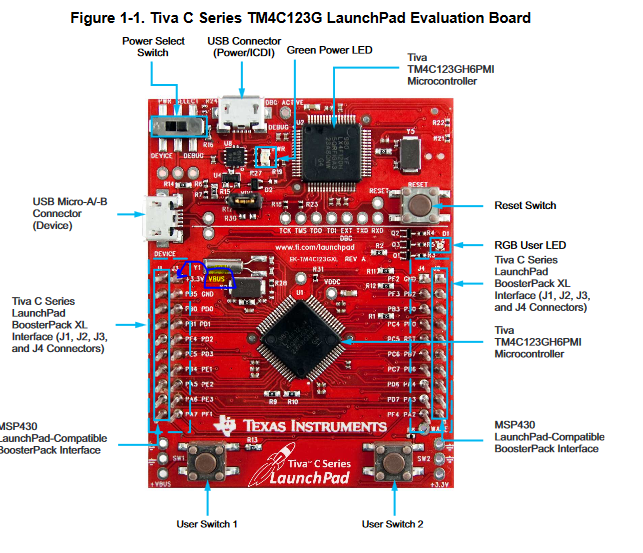
You can connect +5V to J3 pin 1 and GND on J3 pin 2. The schematic is in appendix A of the User's Manual. J3 is shown on page 20. www.ti.com/.../spmu296.pdf
Perhaps you are confusing J3 with J1. J3 pin 1 is shown on the schematic as +VBUS. This is 5V.
From the schematic:
And from the table:
I understand that the silkscreen on the top of the launchpad may be confusing. There was not enough room to print the name a each pin for J1 and J3 next to the corresponding pin, so the names are listed in two columns mimicking the pins themselves. The "+3.3V" refers to the leftmost pin, J1-1. The "VBUS" refers to the next pin, J3-1. I tried to indicate which pin is VBUS in the image below:
*** LIKE *** Terrific detail ... and as there exists a, "chance to misinterpret" the silk-screen ID - your explanation WAS "likely" required...
Firm/I have seen (similar boards) add clarification by employing a, "multi-segment arrow" - which "flows" from the "label" - to the noted pin. (this is done just once)
Note too that there was room to, "Double enter" the "PA7 label" - adding the 2nd "PA7" ID just beneath the physical pin. (i.e. just below bottom pin row, exterior/outside pin column)