This thread has been locked.

If you have a related question, please click the "Ask a related question" button in the top right corner. The newly created question will be automatically linked to this question.

TM4C1294KCPDT: Serious issues USB0 may at times POR MCU plugging in cable eventually destroys MCU

Guru 54628 points
Part Number: TM4C1294KCPDT
Other Parts Discussed in Thread: EK-TM4C1294XL, TPD4S012, , TM4C1294NCPDT, TPS2052B

After a few times plugging in USB0 OTG port cable the entire MCU may suddenly POR for no good reason.

Suspecting VBUS the only 5 volt tolerant pin (PB1) not being protected by a 5v zener diode or even a series resistor to PB1 while plugging cable into USB hub port.

When we follow the TI schematic EK-TM4C1294XL for proper USB port design and destroy two MCU's ($28.00) plus the time to install/remove burned out ones, that is an issue!

Both MCU tested did the very same POR resulting in MCU temperature getting smoking hot over the USB input area, perhaps a sign of poor schematic example for proper USB port layout?

Note worthy TPD4S012 (4 channel) ESD suppressor for USB signals datasheet fails to properly identify pin 1 orientation and uses a bottom pad view of pin 1, no installer on earth can ever see through a plastic chip. The chip is so small that even at 8 diopter magnification one can barely make out a white dot mid center near pin 1 side and a dimple on the opposite corner anyone might assume pin 1, but is not pin 1.

That is according to how TI installed the very same IC on the EK-TM4C1294XL we used to insure the ESD protection chip was installed in the proper orientation.  There is also no reflow or pin soldering temperatures listed in datasheet but we kept air flow below 245*C for 10 seconds. It doesn't have any resistive shorts to ground or any other adjacent pins.

How is a 16v zener TPD4S012 protecting the TM4C1294KCPDT VBUS input?

8.2.2.1 Signal Range on D+, D-, ID and VBUS pins:
The TPD4S012 has 3 pins which support 0 to 5.5 V signals, these are suited for the D+, D–, and ID pins. The
VBUS pin is suitable for the VBUS line, and has the benefit of being tolerant of voltages up to 16 V

  • BTW: Not very fond of how Arrow shipped two test MCU's in 12" X 6" huge black plastic carrier placed in anti static bag placed in 12" x 8" foil like anti moisture bag wrapped by more antistatic bubble wrap placed in to a box. Anyone who understands atoms knows plastic polymers have an inherent electron charge and packaging MCU's in that way may have subjected them to an uneven distribution of surface charges in the hard plastic 40 MCU carrier that could have lead to some sort of unexpected extra phenomena.

    That is the MCU shipping story and sticking to it. Preferably put two such MCU sandwiched between 2" x 2" black/pink anti static fine foam and placed in small anti static bag placed in a much smaller moisture bag finally a small box. Also should used anti static grounded tweezers to pick the chip (not fingers) and place onto antistatic foam. Oddly the MCU chips where not inside antistatic plastic tape real carriers another much safer way to ship two MCU.

  • Does not the VBUS pin working voltage of TPD4S012 (20/24v BDV) seems a bit high to protect GPIO PB1 5v tolerant VBUS analog input?

    We will be testing OnSemi TVS +/-30KV ESD zener and a series 100 ohm R into PB1 to protect MCU power rail and USB0  peripheral from hub port surges on the VBUS pin PB1.

    /cfs-file/__key/communityserver-discussions-components-files/908/ESD-Surge-30kv-5v-USB-VBUS-OnSemi-NSPM0051_2D00_D_2D00_1139451.pdf

  • Hi BP101, the black plastic carriers to which you refer are commonly called JEDEC Matrix trays. While they certainly can be overkill for shipping only two parts, they are commonly used during the manufacturing and handling of ICs. Carbon powder or carbon fiber is added to the mold compound of the trays to make them conductive or static dissipative. The trays are not harmful to your parts. Here is some more information (not from TI): www.topline.tv/JEDEC_Tray.html
  • BP101,
    I am sending your thread to the circuit protection forum experts.
  • BP101-

    I do not think that the TPD4S012 would be causing failures in your MCU. The TPD4S012 provides a shunt path for ESD current, so if the device was failing it would cause the TPD4S012 to short and fail, rather than causing a high current path into your MCU. Can you verify where the failure is occuring? You are correct that if the TPD4S012 is wired incorrectly, it could heat up. 

    I also apologize for the small size of the package making it difficult to see, the small size of our device is a very valuable advantage to many customers.

    Thanks,

    Alec

  • We must have cross threaded this issue as I posted in that forum after you did.
  • Hi Bob,
    Thanks for the article link, makes for a good read.

    >>Carbon fibers or carbon powder is combined into the molding compounds to make ESD safe trays (conductive or dissipative).

    Yet not ESD free as shipping two MCU in such a huge plastic carrier in my opinion is not ESD safe. Perhaps why the first MCU had one LED dimly lit and another fully powered even before any firmware was written into flash memory. Yet DMM ohms check indicated no high resistance shorts between either of the GPIO pin PA2 & PA3 or to other pins on either side.

  • BP101 said:
    not ESD free as shipping two MCU in such a huge plastic carrier in my opinion is not ESD safe.

    Have you not - "Justified your conclusion" - by simply "Restating it?"     Such "trays" are produced in such size - to best carry many such ICs - yet have proven SAFE (often best) for even a few devices.     

    Perhaps you should note that our firm - and SO MANY OTHERS - have for MANY YEARS - received such, "Matrix IC Trays" - from MULTIPLE IC Vendors - with (very few or NO) reported Shipping issues.

    Can "your opinion" (which is neither explained nor justified) - in any manner - compete w/a "Long & Well Studied - then Established Shipment Technique" - employed by (almost) or (even) ALL - such Semi-Vendors?      How do you come to  "your conclusion?"      Your "proof" is most always "anecdotal" - which proves FAR from convincing - or logical...

    The "Tray style" was created in answer to the need to provide adequate physical and ESD protection for the "Fragile, Multi-Leaded Devices" - which they successfully and properly "entomb" - preventing damage to those delicate MCU leads...     The fact that this packaging style - proves so NEW (and unwelcome) to you - does nothing to reduce its  clear effectiveness!

  • New MCU's were shipped sandwiched between soft black antistatic foam inside small ESD safe box wrapped in moisture bag and had same two LED's PA2 & PA3 dimly lit. ROM boot loader external SSIO pins seemingly for full support, why are PA2/3 prior to flashing firmware having this current flow issue?

    The other oddity is the three analog comparators outputs had to be inverted from that which TM4C1294NCPDT required them to be inverted to stop false M0nFault input bit changes. Hence a Panic was being thrown to GUI status flags as if a fault had occurred when no such fault had.
  • Wouldn't that have been a saving grace to MCU 5v tolerant input PB1. Yet the VBUS zener seems to have shorted (open) from the surge that went through it.
  • Hi Bob,

    The EK-TM4C1294XL USB0 OTG port VBUS pin PB1 is not properly protected by the TPD4S012 VBUS pin zener. Four of our launch pads VBUS pins have been seriously degraded, some even seriously over temp the MCU from the very low ohmic resistance PB1 to ground.

    The OTG port design omitted a series resistor to VBUS PB1 and Tiva TM4C129x design guide only source to mention an ESD safe hub for OTG designs requiring protocol signaling of VBUS pin. Might it behoove the community TI add a properly rated part on the OTG port to protect 5 volt tolerant VBUS pin PB1?

    Seemingly TI should review the OTG port design or make the TPD zener more robust so that it actually protects MCU pin PB1. Other industry TVS devices are rated to properly protect VBUS DC line from over voltages, not just ESD events. Some USB hubs imported into the US are not ESD safe, nor were they properly designed to monitor VBUS for over current via TPS2052B or like device. Nor are some computers monitoring VBUS for over current and provide multiple USB ports VBUS power extending out from mother board. Many computer USB ports simply have a 48-100 ohm resistor in series with VBUS +5vdc. So the MCU pin PB1 at best is highly volatile even with minimal protection of TPD4S012.

    Seems to me placing the onus on end users to provide VBUS +5vdc over current or voltage protection is not proper protocol for US engineering!

  • Is there anything else you need on this thread or can it be closed?

    Regards,
    Cameron
  • Hi Cameron,

    I can't find anything wrong with TDP removed from PCB and tested via DMM compared to a new TPD but the ID pin was reading a diode drop in both directions in circuit. Perhaps the VBUS pin was not making continuity with PCB solder pad since it had no in circuit diode drop yet does when removed.

    1. Can that condition cause an undesired issue of DP/DM pins 1&2, removing the ID pin from entering the MCU made no difference? The only other difference is pin 2 trace connects across top surface to pin 5/NC pad, avoids adding a VIA off the side of the ESD trace route path into TPD pin 2. 

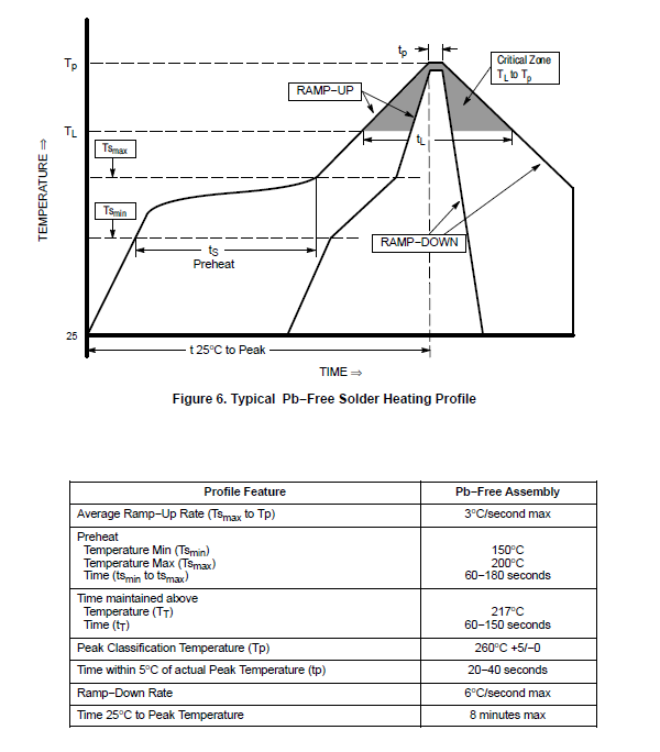
    2. Can you please specify what is the maximum reflow temperature for the TPD device and how long can it be subjected to any peak? 

  • Typical reflow profile for PB free HAL is ok with TPD4S012? With hot air installing new TPD roughly 4+ minutes total time; Preheat 170*C for 2 minutes then ramp up to 258*C over 80 seconds, finally 40- seconds 258*C. The HAL did not reflow TPD onto 2oz CU pads, used no clean liquid rosin prior to preheat. The previous TDP had used 270-280*C above device hot air and it seemed to reflow, it did not easily move with force after. HAL on sides of TPD appeared as if reflow occurred, viewed under 8 diopter magnification.