


Other Parts Discussed in Thread: UCC27714, REF2033, TPS735, INA240, TM4C1294NCPDT
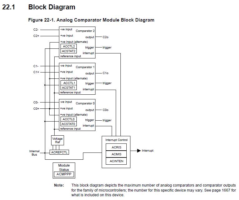
External +VREF threshold is well above input tip point (2.8v) yet most any signal magnitude input -C0,-C2,-C3 @1.24v causes (C0O,C1O,C2O) outputs to toggle.
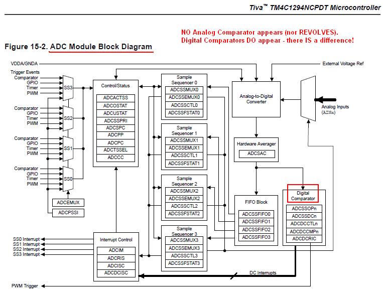
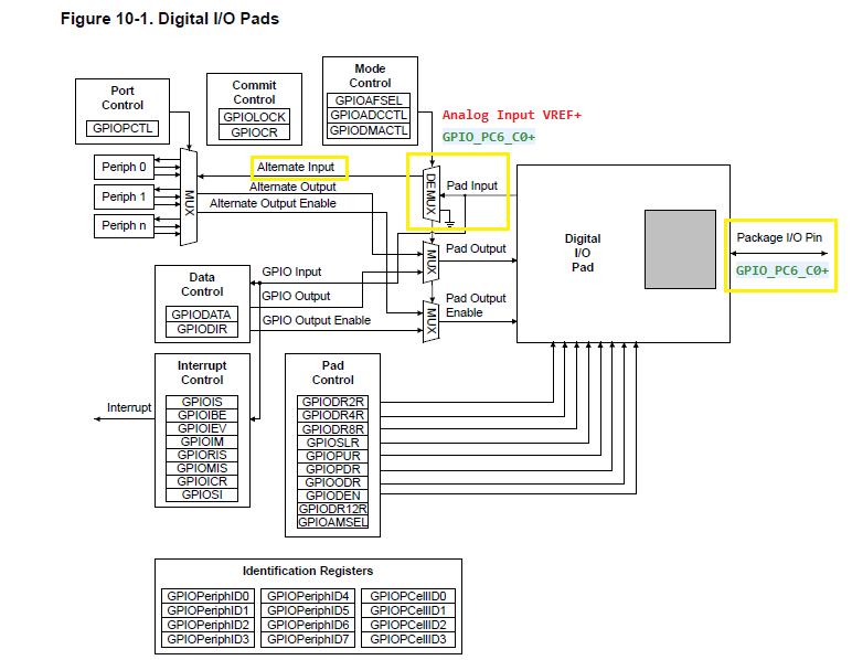
Three analog COMPS use single C0+ source (PC6) setting the input threshold of -C0,-C1,-C2 configured for alternate +VREF C0+,C1+,C2+. Oddly COMP trips too occur below any thresholds of Internal +VREF with ASRCP_REF ladder resistors set for highest values of VREF table 22-3, 22-4. Configuration for Analog COMPS to use external +VREF PINO is shown below.
        //
        // Unlock pin 23 PC6 GPIO for analog PIN0 +VREF.
        // Select the bits to modify in the GPIO commit register.
        //HWREG(GPIO_PORTC_AHB_BASE + GPIO_O_LOCK) = GPIO_LOCK_KEY;
        //HWREG(GPIO_PORTC_AHB_BASE + GPIO_O_CR) &= 0x40;
        // Enable PC6 pin 23 as the external +VREF input.
        //MAP_GPIOPinConfigure(GPIO_PORTC_AHB_BASE);
        /* Alternate +Vref source PC6 pin 23 (C0+input) */
        //MAP_GPIOPinTypeComparator(GPIO_PORTC_AHB_BASE, GPIO_PIN_6);

        /* Configure each ANALGCOMP (+ve0) VIn+ for the
         * C0+ external reference input source */
        MAP_ComparatorConfigure(COMP_BASE, 0 , (COMP_TRIG_NONE |
                                COMP_ASRCP_PIN0  | COMP_OUTPUT_INVERT));
        MAP_ComparatorConfigure(COMP_BASE, 1 , (COMP_TRIG_NONE |
        		                COMP_ASRCP_PIN0 | COMP_OUTPUT_INVERT));
        MAP_ComparatorConfigure(COMP_BASE, 2 , (COMP_TRIG_NONE |
        		                COMP_ASRCP_PIN0 | COMP_OUTPUT_INVERT));
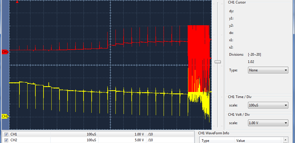
Things get freaky odd when ADC1 SS0/1 are configured for (high speed) trigger source PWM0 versus (low speed) ADCTriggerProcessor() polled 1 second intervals from GPTM interrupt. The actual ADC sampled input signals appear to morph under the same external test conditions. That is to say when the trigger source of ADC1 is slowed down (SS0, SS1) the actual analog input channel signals appear to reduce in magnitude and have fewer or no negative spikes jotting below ground. Those channel signals are derived from monitoring PWM0 module GEN0,1,2 during 20Khz inverter commutation, no motor attached. Part of the issue revolved around UCC27714 not accepting a HI/LI input pulse below 100ns was creating BusVoltage spikes from 24vdc power supply source well above 90V during Cboot PreCharge.
Yet a small motor could be made to run under FOC commutation (7600 RPM), source roughly 400ma from 24VDC switching supply. Startup voltage surge has been corrected via simple tweak of SW though was unexpected TI would change the industry standard gate driver HI/LI rules as to cause mayhem. That motor run is important to note as it proves the MCU driven inverter can produce proper motor commutation yet the Analog COMPS +VREF seems to have other ideas. Yet the Analog COMP fault source outputs C0O,C1O,C2O were disabled in SW to prevent false tripping via external or internal +VREF calibrations. Trying without any luck to correct behavior thus leaving both C0o,C1o,C2o and M0nFault GPIO's disabled.
Three analog COMPS outputs (C0o,C1o,C2o) are enabled and confirmed CCS debug with external +VREF. Yet how can we know GPIO PC6 is actually being configured in the ACEMUX and inputting the external +VREF as expected. How using CCS debug can we verify TP15 +VREF voltage is making way into the C0+ alternate as confirmed in CCS debug?


