This thread has been locked.

If you have a related question, please click the "Ask a related question" button in the top right corner. The newly created question will be automatically linked to this question.

TM4C1294KCPDT: Analog isolation barrier ANIx inputs leak into digital realm

Guru 55913 points
Part Number: TM4C1294KCPDT
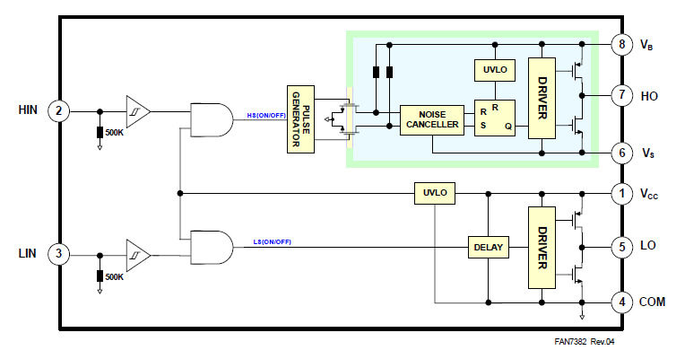
Other Parts Discussed in Thread: UCC27714, LM339,

Register 21: GPIO Analog Mode Select (GPIOAMSEL), offset 0x528

Important: This register is only valid for ports and pins that can be used as ADC AINx inputs. If any pin is to be used as an ADC input, the appropriate bit in GPIOAMSEL must be set to disable the analog isolation circuit. The GPIOAMSEL register controls isolation circuits to the analog side of a unified I/O pad. Because the GPIOs may be driven by a 3.3-V source and affect analog operation, analog circuitry requires isolation from the pins when they are not used in their analog function.

*******************************************************************

Register 10: GPIO Alternate Function Select (GPIOAFSEL), offset 0x420

The GPIOAFSEL register is the mode control select register. If a bit is clear, the pin is used as a GPIO and is controlled by the GPIO registers. Setting a bit in this register configures thecorresponding GPIO line to be controlled by an associated peripheral. Several possible peripheral functions are multiplexed on each GPIO. The GPIO Port Control (GPIOPCTL) register is used to select one of the possible functions.

0 The associated pin functions as a GPIO and is controlled by the GPIO registers.

1 The associated pin functions as a peripheral signal and is controlled by the alternate hardware function.

************************************************************************************************************************

Register 22: GPIO Port Control (GPIOPCTL), offset 0x52C
The GPIOPCTL register is used in conjunction with the GPIOAFSEL register and selects the specific
peripheral signal for each GPIO pin when using the alternate function mode. Most bits in the
GPIOAFSEL register are cleared on reset, therefore most GPIO pins are configured as GPIOs by
default. When a bit is set in the GPIOAFSEL register, the corresponding GPIO signal is controlled
by an associated peripheral. The GPIOPCTL register selects one out of a set of peripheral functions
for each GPIO, providing additional flexibility in signal definition.

So ADC0/1 are not classified as peripherals thereby necessitating setting of AFSEL bits for ANIx input pins?

How did Tivaware peanut butter get into UCC27714 chocolate signals?

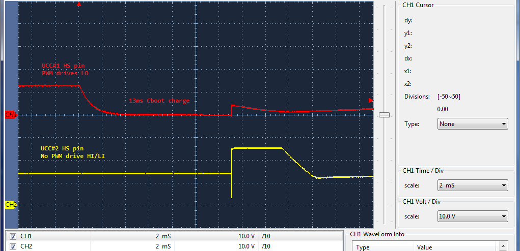
We have been trying to track down how PWM generator pulse periods seem to occur (phantom) on GPIO peripheral pins, when not being instructed by the application. Often these phantom peanut butter pulses are mirror copies of intended chocolate pulses application sent via PWM peripheral configured GPIO pins. The PWM pins action results are being monitored via ANIx channels and Special Analog inputs of the MCU. Peanut butter pulses (sticky) can oddly end up inverted below ground or as a single rouge phantom pulse thus triggering an external device to drive a damaging pulse.  Other TI forum gurus can not understand how such a damaging pulse can occur if the application did not instruct the pulse to be created. Otherwords the peanut butter pulses cause unclassified eratta in the chocolate driven external IC device. 

The evidence of GPIO pin isolation barrier break down is indicated via numerous scope captures. All evidence of barrier break down seems contrary to REG 21 claim that the barrier should be disabled rather than enabled for ANIx pins. Alternatively for special analog device inputs in table 10-2, why would they be any different than ANIx pins?

It would make sense to disable the isolation barrier for digital pins when the DEN bit is set or AFSEL bits set too, for a peripherals digital function. However clearing AFSEL bits (REG10)  suggest a Special pin be under GPIO register control and AMSEL bit being set for ANIx channels disables the isolation circuit barrier.

All ANIx pins appear correctly configured verified CCS debug, according above documentaion. However the MCU analog isolation brarrier is failing to isolate digital I/O from analog inputs for what ever reasons! If AFSEL bits are cleared for ANIx pins does that not remove the isolation barrier in the GPIO unified I/O pad also shared by Digital pins?

Does it not sound odd to disable an analog barrier on ANXi pins or special funciton analog pins?

  • Another added note:

    The circuits PWM digital drive remains isolated from the analog ANIx inputs until there is an external high impedance path completed between them. Voltage magnitude on the analog side a some high level seems to migrate into the digital I/O pad from the analog comparators outputs. When that occurs the MCU will POR without ResetCause register indicating why. 

  • My belief is the GPIOAMSEL bits should be (Set) only for peripherals setting (AFSEL/DEN) bits for (Digital I/O pad pins), thereby disable or (isolate) Digital I/O pads GPIO pins away from Analog I/O pad inputs.

    Tivaware GPIOPinTypeADC() then incorrectly sets REG21 (0x528) GPIOAMSEL bits for ANIx pins inputs of I/O pad which (disables) the isolation barrier between digital I/O pad GPIO and Analog I/O pad inputs.

    That is sort of backwards logic operation most peoples minds but seems to make sense reviewing Figures 10-1/10-2. So the ANIx pins would appear to be working correctly until their is a digital current path involved with them and the analog isolation barrier does not exist on the Digital GPIO pin since it was incorrectly disabled by GPIOPinTypeADC().

  • AKA internal cross talk of the two GPIO I/O pads (Digital||||||||Analog) could randomly occur if the isolation barrier between the two I/O pads has been removed from the ANIx pins.
     
    Seemingly we retain the analog isolation barrier on GPIO Digital pins by telling the Analog I/O pad AMSEL REG 21 to (disconnect) the Digital GPIO pin from it but not set AMSEL bits for the GPIO configured ANIx pins.

  • Hello BP101,

    Alternatively, the issue could be layout related where analog and digital signals aren't fully isolated on your board causes the leakage to occur on traces on your hardware which gives a false impression our device has an issue.

    If you want a TI investigation into this, provide the following:
    1) Prove the occurrence of the issue with either our LaunchPad or DK board
    2) Provide the source code that generates the occurrence of the issue for us to use on our hardware here
    3) Provide the steps taken in measuring the occurrence for us to be able to reliably replicate the failure

    I don't believe you will be able to replicate this issue on our EVM hardware. No other customers have had this issue before for years of use of TivaWare. You can believe what you want regarding TivaWare, but I'll continue to believe that years of customers without an issue like this is proof that TivaWare is not to blame unless you can show me that the issue clearly occurs on our LaunchPad and arm me with a means to replicate it and see it with my own two eyes.
  • HI Ralph,

    Perhaps the wording (disables analog isolation) in REG 21 text is not the best and seemingly stated analog by mistake. The word Digital would be more believable relative to FIG 10-2 and REG21 configuration. Anyway making the only GPIO's driven by a 3v3 source also sharing ANI15,ANI4,ANI13 (PD0-2) inputs are Analog comparators outputs Co1, Co2, Co3. Seemingly they apply to how the REG 21 text is worded since they meet all the qualifications outlined, yet are special analog pins?

    Making 3 comparator outputs analog  setting AMSEL bits with HW direction seems to have destroyed the output pins or the 3 inputs they were connected to, MoFault0-2. I fail to see how FIG10-2 disables analog isolation and makes no sense when the Goal is to enable as much ANIx isolation of the shared 3v3 pins configured as GPIO Digital. Seems like text from another language translated into English makes no sense, poppycock. Seemingly we need to enable digital isolation from shared ANIx pins on the shared I/O pad according to FIG10-1/2 being one and the same I/O pad. Who cares if the silicon does some wacky inverted crap on the I/O pad, the designer only needs to know ANIx pins become isolated from Digital pins when the digital barrier is enabled. That wording becomes critical when tracking down perceived ghosts crossing the I/O pad barrier. And there is still leakage across the isolation barrier even when it is (enabled) so it is not full proof or only protects signal migration to a certain db level or specific voltage potentials.

    Register 21: GPIO Analog Mode Select (GPIOAMSEL), offset 0x528

    Important: This register is only valid for ports and pins that can be used as ADC AINx inputs. If any pin is to be used as an ADC input, the appropriate bit in GPIOAMSEL must be set to disable the analog isolation circuit. The GPIOAMSEL register controls isolation circuits to the analog side of a unified I/O pad. Because the GPIOs may be driven by a 3.3-V source and affect analog operation, analog circuitry requires isolation from the pins when they are not used in their analog function.

  • BTW: There are no analog signals leading into ANI13,14,15 if that was considered above post. The word shared REG21 context does not imply a physical analog connection rather some other peripheral my share the ANIx inputs.

    The loss of analog comparators outputs (Co1,Co2,Co3) when reconfigured back to Digital outputs is interesting.
  • The idea for making Co1,2,3 analog which then sets AMSEL bits for the analog comparators outputs (disables) the analog barrier being they are GPIO 3v3 digital pins.

    The word (disable) does not work well in context of Analog Comparator typically produce an analog output, not digital as it was configured. That was a potential ghost barrier in my mind where AMSEL bits are not being clarified in context of analog comparators divide in the GPIO I/O pad.
  • BP101 said:
    Analog Comparator typically produce an analog output, not digital as it was configured.

    Have you "ANY BASIS - WHATSOEVER" for that  "Not Digital" reach?     Kindly present (any) published proof - in support of (your) "opinion."

    Is it not true - instead  - that  EVERY Analog Comparator "Commercially  Produced" - is equipped  INSTEAD with a  DIGITAL OUTPUT!    

    The highest selling  Analog Comparator of  "All time"  the venerable LM339 -  has employed  FOREVER - ALWAYS & ONLY - DIGITAL OUTPUTS  (4 of them) and  ANALOG INPUTS.    As too - every single Analog Comparator - w/in the (multiple) data-books - at firm's/my disposal.    

    MCUs here - have not "Migrated from that,  "Analog Comparators produce DIGITAL OUTPUT" standard!     Why possibly - would they - to what advantage?    (to SO break from convention!)

    Presented here are the API's "Proof Positive, MCU configurations"  clearly confirming that Analog Comparator Outputs (even w/in an MCU) are to REMAIN  "DIGITAL."

    void GPIOPinTypeComparator(uint32_t ui32Port, uint8_t ui8Pins)    //  Note this treats the Analog Comparator's INPUTS!
    {
    // Check the arguments.
    //
    ASSERT(_GPIOBaseValid(ui32Port));
    //
    // Make the pin(s) be inputs.
    //
    GPIODirModeSet(ui32Port, ui8Pins, GPIO_DIR_MODE_IN);
    //
    // Set the pad(s) for analog operation.
    //
    GPIOPadConfigSet(ui32Port, ui8Pins, GPIO_STRENGTH_2MA, GPIO_PIN_TYPE_ANALOG);
    }

    Yet the Analog Comparator's OUTPUT:

    void GPIOPinTypeComparatorOutput(uint32_t ui32Port, uint8_t ui8Pins)
    {
    //
    // Check the arguments.
    //
    ASSERT(_GPIOBaseValid(ui32Port));

    // Make the pin(s) be inputs.                 // Note - "OUTPUTS" this is a "Copy/Paste Error" - carried over (almost certainly) from the function (above.)
    //
    GPIODirModeSet(ui32Port, ui8Pins, GPIO_DIR_MODE_HW);

    // Set the pad(s) for standard push-pull operation.
    //
    GPIOPadConfigSet(ui32Port, ui8Pins, GPIO_STRENGTH_2MA,  GPIO_PIN_TYPE_STD);      // keywords "Push-Pull" & "GPIO_PIN_TYPE_STD" clearly signals  DIGITAL OUTPUT!
    }

  • It would seem you are attempting to steer the topic in another direction versus discussing how analog GPIO barrier is being disabled from signal migration onto analog comparators output and in to the digital realm. Don't believe the analog comparator section of TM4C1294x datasheet states the comparator output is either digital or linear by design.

    The point was also made the analog comparator did not need to have inputs configured by GPIOPinTypeComparator() and functions after calling ComparatorCOnfigure(). Thus it would seem the analog comparator must follow the very same configuration rules as ANIx inputs if any part of the comparator is shared with analog I/O pad as the outputs do. Analog isolation disabling has not been done in any Tivaware calls for the comparator output.

    For the context of the thread "Analog isolation barrier leaks" the comparator output was thought to be more LINEAR and not GPIO digital as it was configured. In the context of an MCU, analog comparator the digital output would mandate binary logic levels are being produced which is not shown in electrical specifications section of datasheet.

    LM339 comparator output does not produce binary digital (1/0) logic signals, outputs are often TTL, yet they always seemed more linear like me.   

  • The problem causing analog isolation barrier migration was discovered this weekend to be restriction of PWM pulses <100ns of UCC27714 HI/LI inputs. PWM pulse widths below 100ns causes it to produce high voltage and POR's the MCU around 90vdc. Trying to PWM UCC @1% duty cycle quickly POR's MCU in the first 5ms of PWM drive. That is called slow NFET decay in the BLDC world and who would have believed UCC27714 could be so destructive to TM4C1294 MCU.

    Most other vendors do not have <100ns pulse input block on their gate drivers as TI has for some reason put into UCC27714. That has caused hours of added delay where no delay should have been. Fact is it required SysCtrlDelay() in Cboot charge cycles slowing 20Khz PWM down to 333Hz or MUC would POR simply doing that part.
  • BP101 said:
    LM339 comparator output does not produce binary digital (1/0) logic signals, outputs are often TTL, yet they always seemed more linear like me. 

    So - you now promote  "TTL Outputs"  from Digital - to Analog?    Of course - that is (also) patently UNTRUE.     Without ANY DOUBT - LM339 produces binary, digital (1/0) Outputs!

    LM339 outputs are "open Collector" -  thus a pull-up is required for the output to "register as logic high" - and always and only - assumes the voltage level of the pull-up - provided the output is not (excessively) loaded.     Those outputs - in no way - are confined to TTL levels!     

    You may be "confusing" the behavior of Analog Comparators with Operational Amplifiers.      Multiple texts are available - to (better) inform you...

    That said - your continued "misstatements" - memorialzed here -  and (easily checked/verified) should NOT pass w/out proper challenge!     Should not (some) time be spent investigating - prior to making so mistaken (and continuing)  statements?

  • Our sources have resolved that high voltage is being generated by the UCC27714 gate driver behavior toward MCU generated PWM pulse widths. If the MCU application allows the magnitude to grow unconstrained the MUC will POR when the magnitude reaches a certain trip point. That is how TM4C1294KCPDT analog I/O pad barrier is being corrupted, not from PCB design.

    Ideally a proven application successfully working via other vendors gate drivers should not have to be the baby sitter of TI gate drivers. Nor should anyone ever have to do an application rewrite as a work around for oddly preforming gate drivers. Seemingly vendors should try to keep consistent gate driver characteristics uniform for MCU driven PWM signals and not attempt to restrict basic industry accepted PWM signal behavior for what ever the reasons.

    Below you will see how PWM inverter voltage gain cause the analog barrier trip point to occur. Capture show MCU driven PWM pulse width corruption via UCC27714 gate drivers HI/LI inputs being restricted >100ns pulse widths. If you have an easy WA for this behavior please post duty cycle update function that can produce slow decay inverter current without producing a PWM pulse width <100ns. So far all attempts have been futile and painfully driven on our part, hundreds of unexpected candle hours burning to make such work via UCC27714 drivers.

  • One view is digital binary levels are not the same as TTL driven logic and 3v3 TTL does not define a binary high/low digital voltage levels either. So to say the LM339 produces digital output levels on it's own accord is not entirely correct. You point out it requires resistor pull up and mating 3v3 input to accomplish a level shift ability. Still recall the output has linear drive capability too based on the configuration and input signal.

    You may have touched on something more important! Previously had set WPD on MCU analog comparator output, perhaps should have made set for WPU. There is not a fair amount of info on the entire MCU analog comparator configuration of GPIO I/O pad and analog barrier totally skirted over in any register configuration.

    Why are we left to assume the Analog Comparator exists in the analog barrier and silicon disabled output of the digital I/O pad?
  • Indeed - the use of a "Pull-Up" for (most) Analog Comparators' Outputs is (reasonably) standard.

    That same pull-up R "cannot hurt here" - yet our LX4F and 4C123 Analog Comparators - have been able to toggle high - without requiring use of (any) pull-up!      The "switch" from logic low - to logic high - occurs w/out fail - whenever  the voltage upon the non-inverting input (+) exceeds the voltage upon the inverting input (-).    

    Again - as I  STRIVE to provide "Printed Fact" - to "back-up" my viewpoints (something "others" should adopt) - I will present AGAIN - that earlier presented.    (in YOUR exclusive behalf!)

    void GPIOPinTypeComparatorOutput(uint32_t ui32Port, uint8_t ui8Pins)

    {

         // Check the arguments.

          ASSERT(_GPIOBaseValid(ui32Port));

          // Make the pin(s) be inputs.    (Outputs)            //   Again - as earlier noted - "input" here is a clear - "Cut/Paste" error.    (copied surely - from the Comparator (input) function.)

          GPIODirModeSet(ui32Port, ui8Pins, GPIO_DIR_MODE_HW);

          // Set the pad(s) for standard push-pull operation.

          GPIOPadConfigSet(ui32Port, ui8Pins, GPIO_STRENGTH_2MA, GPIO_PIN_TYPE_STD);

    }

    Might your "Attention to Detail" require (some) slight improvement?    The above - sent to you a few hours earlier!    

    "Push-Pull" - as well as "GPIO_PIN_TYPE_STD"  -  signal without doubt - that  the Analog Comparator Output is Digital - and in NO NEED of any pull-up resistor!

  • And again you evade any questions to the analog comparator isolation barrier inputs do not requiring additional Tivaware calls other than ComparatorConfigure() in order to function. Yet many add the GPIOPinTypeComparator() / GPIOPinConfigure() calls as being required without question. SW engineers apparently rushed to conclusion never tested Analog comparator inputs default same as ANIx analog I/O pad. Again that brings to question WHY and how is the analog isolation barrier being configured (disabled) in the GPIOAMSEL REG 21 bits? How has the MCU analog comparator escaped the AMSEL bit programming of analog I/O pad, (required configuration ANix pins) so the GPIO pin output becomes isolated from the analog inputs?

    One can not simply pick the part they want to dispute and disregard all other points being made in a debate as being non valid. Is that not how politicians attempt to discredit all other points as being non valid to a discussion? Perhaps one could say that might have escaped the attention of Tivaware SW engineers, as we are all human and make mistakes.

    Accepting without question what someone else has done via SW calls as being completely factual may lead to poor outcomes, when TM4C1294x datasheet is not being specific on the topic. Do we automatically assume the MCU analog comparator has not an open collector output and is designed digital when that point has not been verified by datasheet text?

    Below a popular comparator PDF, attention to detail may have escaped an earlier jump to conclusion that comparators must have digital outputs. You will discover an OP amp configuration which is very linear in behavior and has open collector outputs.

    /cfs-file/__key/communityserver-discussions-components-files/908/Comparator-quad-low-single-supply-NJM2901_5F00_E.pdf

  • BTW:
    The capture above CH2 appears to be shoot through on B phase caused by LO outputs firing while HO outputs do very same thereby disrupting Cboot charges in each HO/HS cycle. DMM measures 38K ohms resistance between any 2 of 6 PWM pins and traces well isolated via GND plane decoupled at HI/LI inputs of three UCC27714. Somehow PWM GEN1 A/B pulses must be randomly occurring together, not always coincident. Scope capture this AM has caught the center UCC HO/LO outputs producing random 1us output pulses 100us apart in side a 900us frame.

    All 6 PWM traces were tested for high impedance cross talk (shorts) prior to population of any IC by vendor and us both testing PCB traces. Again DMM can not detect any odd resistance reading across PWM GEN1 pins. So either the UCC is defective or is being commanded my MCU to produce random mirror pulses on GEN1 output relative to GPIO M0Fault inputs which are OR'd together from Analog comparator outputs.
  • BP101 said:
    And again you evade any questions to the analog comparator  isolation barrier inputs do not requiring additional Tivaware calls

    Indeed - and deliberately so - as I choose to CORRECT (ONE) MAJOR Misstatement - at a time!    So that - just maybe - that correction will be accepted & sink in!    (to YOUR benefit of course - it is YOU who complains that vendor's  Analog  Comparator is "flawed" - when in fact - the (real) flaw is your,  "misunderstanding.")      

    Analog Comparators - always and only - produce DIGITAL OUTPUTS.     Just as the LM339 always HAS!

    As to  your,  "Isolation Barrier" claim - Vendor's Ralph clearly requested, "normal/customary" Supporting Data/Documentation - which you (completely)  [your word now] EVADED!    I don't believe that  you've made (much) case - at all - in support of  (any)  such "Isolation Barrier" issue!      

    Ralph made a generous offer - historically (as witnessed here)  you "refrain" from "honoring" such  "reasonable"  vendor request!"    Is that not - extremely TELLING?

  • cb1_mobile said:
    Indeed - and deliberately so - as I choose to CORRECT (ONE) MAJOR Misstatement - at a time!    So that - just maybe - that correction will be accepted & sink in!    (to YOUR benefit of course - it is YOU who complains that vendor's  Analog  Comparator is "flawed" - when in fact - the (real) flaw is your,  "misunderstanding.")      

    There is no flaw in my understanding only that you too kept insisting all Tivaware configure analog comparator calls were necessary, as we too had believed according to typical configuration of past. Neither has that risen to this vendors attention by evading simple questions they should have answers, provided they are working for TI and have access to this information.

    Either the barrier is disabled for all special analog devices that can use ANIx pins and are constrained by the analog I/O pad or not at all. There is no in-between answers to that simple question, being avoided by this vendor and CB1 does not have enough datasheet disclosure to answer either. No one can blame you for that yet asked for you to think outside the box for this answer as it may lead to some larger discovery. So far it would seem the PWM peripheral MoFault inputs TM4C1294 are not being masked by I/O pad analog protection barrier and signals are perhaps disrupting the PWM generators. That is difficult to know for sure at this juncture but is quickly becoming a possibility to consider in light of recent events occurring around UCC27714 gate driver.

    What supporting data/documentation should a customer have to provide when they are the one asking simple questions about MCU Register configuration vendor should be able to quickly answer. If they can not answer this question relative to analog compactors configuration perceived as NOT being isolated by I/O pad in previous Tivaware calls, perhaps it is because TM4C MCU's are second party sourced and not developed by TI at all. Or they are trying to be over protective and creating customer dissatisfaction on several levels.

  • BTW have discovered TI engineer may have reversed two pins UCC27714 gate driver (HS/HB) in datasheet or has incorrectly drawn HO driver Totem pole PFET top, should exist bottom where NFET is drawn. If Q' were driving HO it would not matter but it is not drawn that way, power device forum Derek also made notice but said it may be incorrectly drawn.

    Why is that important, for one the high side RS latch shows Q not Q' relative to typical industry designs well before TI ever developed any such gate drivers. Hence the PWM generators outputs seemingly must be inverted to compensate for this TI design error.

    Only a lunatic would ever consider inverting PWM signals in high voltage PWM input signals as typical designs avoid inverted PWM like the black plague.

  • Typical industry gate driver has High side PFET on Totem pole bottom, not PFET on top or uses Q' to drive Totem pole if driver FETS are reversed.  Trouble shooting difficult issues is often a process of elimination of the most obvious being first, less obvious later as human awareness takes over. So UCC27714 VB or HB would be VS but is HB instead relative to HI/LI PWM signals. That is of course if the UCC27714 was drawn incorrectly as it was earlier expressed Q should have been Q' in drawing but seems more bamboozling is in play.

  • The top gate driver above post is proven to work with TM4C1294 PWM and not POR the MCU when PWM durty cycle is near 1% or pulse width falls below 100ns.

    Not one word in UCC27714 datasheet that it differs from industry standard PWM signals and may require INVERTED PWM signals to drive HI/LI inputs.

    So we are not to far off in this thread when saying PWM peripheral signals seem to cause negative PWM Ghosts on the analog I/O pad barrier into MCU digital realm.
  • Hello BP101,

    BP101 said:
    Tivaware GPIOPinTypeADC() then incorrectly sets REG21 (0x528) GPIOAMSEL bits for ANIx pins inputs of I/O pad which (disables) the isolation barrier between digital I/O pad GPIO and Analog I/O pad inputs.

    BP101 said:
    Either the barrier is disabled for all special analog devices that can use ANIx pins and are constrained by the analog I/O pad or not at all.

    From the Datasheet: "If any pin is to be used as an ADC input, the appropriate bit in the GPIOAMSEL register must be set to disable the analog isolation circuit."

    If the pin is used as an analog input, TivaWare correctly ensures that the Isolation circuit is disabled. From what I can see this should apply to comparator INPUTs as well, and though it isn't explicitly stated in the DS that is reflected in TivaWare API's for Comparator input configuration GPIOPinTypeComparator.

    For Comparator OUTPUT, that output is DIGITAL (as cb1 has been repeating), and the Isolation Barrier should be enabled - which is why GPIOPinTypeComparatorOutput API exists.

  • Where are you CB1 getting information in datasheet section 22 Analog Comparator have digital outputs?

    GPIO section of datasheet REG21 note also says "if an ANIx can be used" by GPIO ports/pins which are (Co1,Co2,Co3) TTL output structure and is not disclosed how output pins are disabled in the AMSEL REG21 or why they do not need to be disabled being behind analog inputs that share the pin/port ROW in Table 10-2, even though not configured as ANIx pins. The analog isolation barrier is enabled on the un-configured ANIx pins which (Co1,Co2,Co3) use and would be disabled in AMSEL bits if the ANIx pin/port on that row were configured as inputs.

    Setting the analog comparators output as digital does not disable AMSEL bits creating the analog isolation barrier between the analog comparator (+/- inputs) and GPIO outputs. That means the Co1,Co2,Co3 are wide open to analog signals in the analog/digital (shared) I/O pads of un-configured (ANi13, Ani14, Ani15). ANix pins default onto the GPIO analog I/O pad, configured or not! That is how the text can be read as Note first states GPIO Port or Pins before it states being used as ANIx inputs.

    Perhaps Table 10-2 is not properly drawn for the analog comparator inputs/outputs. How can Analog comparator input (type analog) port/pins escape from being disabled in the AMSEL register the only way of enabling the GPIO digital output barrier in the disabled analog I/O pad for that pin/port. Unless configuring a pin as GPIO port/pin disables the analog barrier (by default) which seemingly is not mentioned section 10 or any of the GPIO registers class of service?

    Believing a comparators output is only a digital structure even when TTL coupling can exist may simply be wrong 95% of the time! You could not create OP amps as New Japan Radio's comparator PDF shows if they were purely digital, so comparator outputs can be linear acting and not truly digital as many levels shifts can exist, not simply 1/0 digital binary logic levels.
  • Since you seem to have long forgot, e2e.ti.com/.../1512826 - Amit clearly states this in a past thread from you...
  • Figure 22-2 structure of analog comparator dotted lines in my mind defines the analog I/O pad barrier prior to the output linear signal level magically being shifted into the digital realm via addition Exclusive OR gate. Yet well before GPIO pin output being defined by Tivaware in the I/O pad.

    Figure 22-2 does not paint a well defined point of how the linear part of the comparator output is being isolated from the Exclusive Or gate digital part inside the shared I/O pad. Fig 22-2 also does not regard Tivaware calls as playing any part of the analog isolation barrier being disabled in the I/O pad.