This thread has been locked.

If you have a related question, please click the "Ask a related question" button in the top right corner. The newly created question will be automatically linked to this question.

TM4C1294KCPDT: problems with GPIO-Pins (open drain) at low temperature

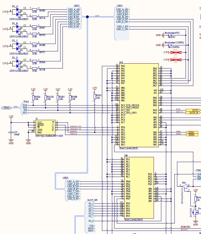
Part Number: TM4C1294KCPDT

Hello everyboby,

my design using a TM4C1294KCPDT uses GPIOs:

*  on GPIOs (PM and PK) initialized as OD-Outputs I have LEDs connected (3.3V --> LED --> Resistor 330R --> GPIO)

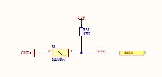
*  on GPIO (PE) initialized as Input (no PU no PD)  I have connected a reed-Relais ( 3.3V --> Resistor 47K --> GPIO --> reed --> GND)

and I has this problem:

*  at low temperatures (-20°C) the LEDs glow when the GPIO is configured as Output OD and data register is set to high. If this GPIOs are configured as Output Push/Pull the LEDs work as expected.

*  at low temperatures (-20°C) the signal at the GPIO input (reed) is measured as 0.3V even if the reed isn't active. I measure this directly an the controller pin. It seens to me as if this input pin changes to lowstate-ouput-pin.

both effects disapears at 'normal' temperature.

someboby has an idea?

thanks Andres

  • Do you have a schematic showing your connections? Do you have pulls disabled on the GPIO pins driving the LEDs? In general, the pulls are stronger and input leakage is lower at cold temperatures.
  • Bob,

    thank you for your fast reply.

    yes, PUs are disabled for all GPIOs.

    this is the schematic:


    The jumper JB are not set. R38, R39 ar not fitted.

    The effect on the input for signal /REED on PE2 begins at the same 'time of coldness' as the LEDs begin to glow. After warming the board to 'normal' temperature the LEDs work in the right manner but the REED-input continue stacking for ca. 1-2 hours at low signal. Measuring the REED-contact I get an open switch ( 00-OHMs) all the time but the voltage at the Input pin is 0.3V. After this time, the REED-input works ok and without any faults. All the time a little testprogram runs blinking the LEDs and checking the REED-input to be high.

  • May I note the, "ADDED CONFIDENCE" which would accompany your (rather detailed) report - should you confirm your findings - ACROSS SEVERAL ADDITIONAL BOARDS!

    Single Board Anomalies simply, "EAT TIME & EFFORT" - far out of proportion - to their worth.

    How did you "Clean your boards?" Certain "cleaners" enable "unwanted residue to linger" - which (may) amplify (or at least add to) what you've noted...

    As a (very) Quick/Dirty Check - might your duplication of your GPIO "Hook-Up" - but moved to the closest matching, "Vendor Eval Board" - provide additional (possibly insightful) data?

    I can note that several of our  "TM4C123 board designs" - riding on "weather balloons/similar" (at altitude) - have functioned well - at (even) lower temperatures...

  • Hi Andres,
    I do not see the schematic.
  •   Bob,

    something hasn't work with the attachments, here the schematics as attached files

  • It is noted that you've tied many (assumed unused) pins together - across multiple ports.     The MCU manual directs that these pins (preferably) connect to Ground.     Undescribed is how your software configures those pins - the default mode orders these to "Inputs."    (I believe that to be safe.)

    Firm/I have noted (somewhat) similar "temperature effects" - which (more significantly impact) these MCU circuits/sections:

    • VDDC - the external capacitors - which tie to these two pins - must maintain their capacity @ low temperatures
    • the external crystal / support components (caps) must be spec'ed for - and maintain performance - as well

    We find it useful to monitor "ALL" MCU voltages when such "irregularities are noted."    (i.e. especially as you approach the -20°C "distress zone.")     In addition - monitoring  the MCU's current draw - again especially near the, "distress zone" - often proves useful.

    Again - you remain  silent as to the "Number of Boards" which exhibit this condition.    Your case amplifies - when the issue appears - (beyond) once!

    In addition - if only for (temporary) test purposes - having several pins output at known frequency (100KHz suggested) & duty cycle - and then "observing for deviation as the temperature drops" - proves of  significant  value...    Timer pins - w/Timer set to "PWM Mode" - prove quick/easy (i.e. "meant") for such purpose!      

    We note you have a, "little test program" - yet the method suggested here - being  "Deliberately more quantitative / less coarse" - is  better able to "Detect & Note" any such  "onset of disturbance..."    (even if - and especially if - the disturbance is "slight.")

  • I don't see anything obvious in the schematic. If you put a board with no software (erased flash) powered up at -20C, do you still see the LEDs glow?
  • Would not such "test" ... under "no software/erased flash" conditions - prove, "Less than compelling" - as the GPIO (may) "awake" into GPIO INPUT Mode? (i.e. Is the "Raw, unprogrammed device" guaranteed to exhibit (any) expected default, pin management?)

    It (must) be assumed that the cascade of (earlier) and (proven) diagnostic suggestions - were "dismissed" for (some) reason - that's fine (although perhaps "Less than Wise") yet it would be useful to (really) KNOW!

    Should it be "forgotten" that poster's initial post  "opened" with,   "Hello EVERYBODY!"     

  • I have not heard back from you. Have you resolved this issue?
  • Bob,

    I have decided to see the problem as solved.

    This problem appears if only the CPU-chip was cooled heavy with a cooler spray and the other area of the board are at 'normal' temperature. This is not an really existent working point for the whole system and we observed the errors doing stress-test with a few prototypes.

    Thank for your help!