This thread has been locked.

If you have a related question, please click the "Ask a related question" button in the top right corner. The newly created question will be automatically linked to this question.

TM4C129XNCZAD: strange SPI bus output after switching data widths

Part Number: TM4C129XNCZAD

I have been beating my head against the wall for several days trying to figure out what could be going wrong with my SPI bus communication. I use a single bus to talk with two different devices. Device A uses an 8-bit data width, and device B uses 16-bit data width.

If I never talk with device B, the communication with device A works fine. But if I talk to device B and then switch to device A. I get an odd behavior.

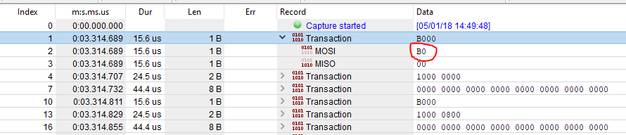
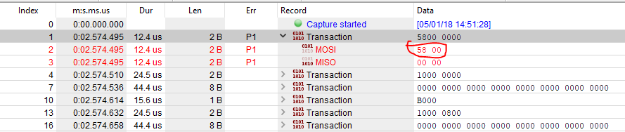
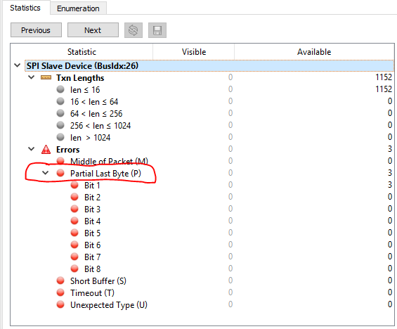
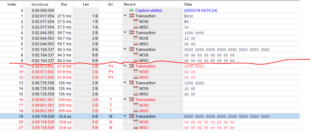
I am using a Beagle SPI bus sniffer to examine the data that is being transferred between the Tiva and device A. When I send a command code of 0xB0 to device A, the sniffer shows that one byte containing the proper value is being transmitted. If, however, I talk with device B first, when I reconfigure the SPI to 8-bit mode and send the 0xB0 to device A, the sniffer indicates that 2 bytes were sent -- 0x58 and 0x00. It is interesting that 0x58 is 0xB0 shifted right by one bit. The sniffer also flags a "partial last byte" error for the transaction. Subsequent transactions seem to be okay.

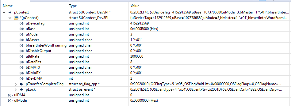
I checked the contents of the SSI registers just prior to transmission in both cases (before talking to device B and after), and they are identical:

SSI_CR0 0x000013C7  SSI Control 0 [Memory Mapped]   
    SSI_CR0_SCR 00010011    SSI Serial Clock Rate   
    SSI_CR0_SPH 1   SSI Serial Clock Phase  
    SSI_CR0_SPO 1   SSI Serial Clock Polarity   
    SSI_CR0_FRF 00 -    SSI Frame Format Select 
    SSI_CR0_DSS 0111 -  SSI Data Size Select    
SSI_CR1 0x00000000  SSI Control 1 [Memory Mapped]   
    SSI_CR1_EOM 0   Stop Frame (End of Message) 
    SSI_CR1_FSSHLDFRM   0   FSS Hold Frame  
    SSI_CR1_HSCLKEN 0   High Speed Clock Enable 
    SSI_CR1_DIR 0   SSI Direction of Operation  
    SSI_CR1_MODE    00 -    SSI Mode    
    SSI_CR1_EOT 0   End of Transmission 
    SSI_CR1_MS  0   SSI Master/Slave Select 
    SSI_CR1_SSE 0   SSI Synchronous Serial Port Enable  
    SSI_CR1_LBM 0   SSI Loopback Mode   
SSI_DR  0x00000000  SSI Data [Memory Mapped]    
SSI_SR  0x00000003  SSI Status [Memory Mapped]  
    SSI_SR_BSY  0   SSI Busy Bit    
    SSI_SR_RFF  0   SSI Receive FIFO Full   
    SSI_SR_RNE  0   SSI Receive FIFO Not Empty  
    SSI_SR_TNF  1   SSI Transmit FIFO Not Full  
    SSI_SR_TFE  1   SSI Transmit FIFO Empty 
SSI_CPSR    0x00000002  SSI Clock Prescale [Memory Mapped]  
SSI_IM  0x00000000  SSI Interrupt Mask [Memory Mapped]  
SSI_RIS 0x00000048  SSI Raw Interrupt Status [Memory Mapped]    
SSI_MIS 0x00000000  SSI Masked Interrupt Status [Memory Mapped] 
SSI_ICR 0x00000000  SSI Interrupt Clear [Memory Mapped] 
SSI_DMACTL  0x00000000  SSI DMA Control [Memory Mapped] 
SSI_PP  0x0000000D  SSI Peripheral Properties [Memory Mapped]   
SSI_CC  0x00000000  SSI Clock Configuration [Memory Mapped] 

Do you have any idea how, given that the SSI registers are the same in both cases, different behaviors are observed? And is there anything you can suggest I look at for more clues, or any possible workaround for this problem?

Regards,

Dave

  • Surely the vendor will suggest that you, "Employ the API" - which provides many examples - although NONE which venture into your (rather unique) terrain.

    I would BET that your implementing an "MCU SPI Peripheral RESET" - upon each, "Change from "8 to 16" (or vice versa) would correct - yet such IS (admittedly) extreme!

    It IS "Good to note" that your "measuring instrument" - clearly - played NO PART in what you (now) report.

    Your (even if temporary) use of the API - just to see if such "May Resolve" - seems reasonable for the added insight - it (may) provide...

  • Hi, cb1,

    I am already using the TivaWare API functions to set everything up and do the data writes and reads. I did try doing a simple test in loopback mode where I just changed the data width back and forth, but I could not reproduce the problem. So there may be something else going on besides just data width, although I cannot see what it might be at the moment.

    Your suggestion of competely resetting the SSI peripheral is worth trying as a diagnostic tool. But as you say, it is a bit extreme for real-time operation.

    Regards,

    Dave
  • As cb1 suggested, I tried doing a full reset of the SSI peripheral just before writing to device A:

    SysCtlPeripheralReset(SYSCTL_PERIPH_SSI3);
    while (!SysCtlPeripheralReady( SYSCTL_PERIPH_SSI3 ))
    {
    }

    This actually made things worse. It causes the same incorrect behavior (transmitting 0x58, 0x00), but without having talked with Device B! I suppose this is a good clue, but it sure seems to defy logic. Perhaps a night's sleep will make things clearer to me.

    Regards,

    Dave
  • [edit] kindly note that Dave's post (17:20) and mine (17:21) just crossed!     (the writing below - had NO AWARENESS of Dave's recent findings)    The [edit] portion (blue) has such awareness!

    Hi Dave,

    I agree - yet as a Sailor (both myself & vendor's Bob) ... "Any Port in a Storm" (i.e. dreaded Periph. Reset) proves welcome.

    My firm generally finds - that once we can achieve (some) success - usually (complete) success - is far "faster/easier" attained.    I don't believe any but the "most dedicated vendor agent" would "comb thru your DRM Code" - to try to "Tease Out" (your) answer.    I've been at this forum (several others too) and have "NEVER" noted the issue you've described.

    It would have been IDEAL - had your "FOUR DEVICES" been equally "split" - so that those of "like data width" - could co-exist.    

    As an alternative to a "Complete Peripheral Reset" - perhaps you could employ, "Repeated SPI Bus Configuration" - to (maybe) insure that your "change" ... really did take effect!

    And another thought - have you employed the "Peripheral Ready Function" - so as not to "assume" the Bus Config. executed - but to "insure" that it did? THAT - may be the superior suggestion - from this post's barrage...

    [edit}   After reading your latest post (one above):   I see that you DID deploy the "Peripheral Ready" function - at least at "one point" - w/in your latest posting.

    I MUST rise to the defense of  the "Peripheral Reset Function" - to fail - as you note - when such function is "Guaranteed to place the peripheral in a proper & neutral state" almost insures that (somewhere) your Set-Up and Config of the SPI Peripheral - is IMPROPER!    Of that I have NO DOUBT!  

    Now your code indeed shows the "Peripheral Reset()" - but does not, "Show the Required INITIALIZATION (RE-INITIALIZATION) OF THE SPI PERIPHERAL!     Had that (really) occurred?    It IS VITAL!

    I would add - even beyond your "faith in the Beagle Board" - that a nicely legible, "Scope-Cap" - displaying at minimum - two SPI Bytes in frame - would prove GREATLY HELPFUL!    Note too - that you must "Manually Control the CS Line - to each/every  individual Slave Device.    (this proves true especially during your attempt to, "Produce a "Multi-Byte" SPI Transfer!")    I cannot recall if this was past mentioned - yet it IS worth the restatement...

    It is NOT unusual that a "likely" rushed code addition - "misses some critical part" - and it is SURE that the "Peripheral Reset" - followed by PROPER Peripheral Initialization - ALWAYS WORKS!

  • Hi,  cb1,

    The SPI bus is, indeed, re-configured before each use. And yes, the chip select line is being enabled when talking to the devices. The code is known to work correctly on a Stellaris processor. I have gotten stuck with the job of porting it to a Tiva. The only difference is that the interface has moved from SSI0 to SSI3.

    I did not show the setup code, in part because the actual source code uses multiple layers of abstraction, and the calls to the TivaWare library are passed values stored in context structures. So even if I showed the code it would be impossible to see what is actually being configured. That is why I chose to include the actual SSI register contents in my initial post. You can see exactly how the device was configured.

    The troubling thing to me is that the device configuration is exactly the same in both the case that works properly and the case that doesn't. The flags show that both the TX and RX FIFOs are empty. So why do things work differently? Is there something beyond the SSI registers that also impacts the operation of the peripheral? (Note that I am not using DMA or interrupts in this implementation.)

    I will continue to look into the oddity I found regarding the peripheral reset, and post any findings.

    Regards,

    Dave

  • Feel your pain - yet NOT to the degree you surely do.

    Is it possible that the SPI Registers you are monitoring (I suppose via the IDE) are "Read Sensitive" - and the simple fact that those registers are "addressed" - has "masked their content?"    (I don't do much coding any longer - staff proves superior in that area... and we deploy ARM MCUs from three vendors - beyond this one.)

    "KISS" - to which I am addicted - dictates that you, "Start your test/verification process" at the slowest possible data rates.    Even though your slaves (appear) to function (sometimes) - I'd much prefer your moving to the slowest rate - until the issue is properly identified & resolved.

    To the Slave Chip Selects - you do realize that - dictated by the Slave - you may have to, "Command that individual "CS" to remain "active" throughout the  entirety - of your "Multi-Byte" Transaction.     (this is why the "FSS pin (MCU Controlled mode)" sees limited use...)

    While inconvenient - especially if you're "In the Field" - the requested Scope Caps - clearly revealing a "Two Byte" (failed) transaction - would prove of  immense value.     (I'm certain vendor staff - would agree.)   Serial Interfaces are compelling - but a "nightmare" - when failing & proper test gear is "Not Available."    My firm employs multiple Tek Portable Scopes (isolated channels & battery powered) when we "Venture into the Field."      (I don't believe the Beagle Board - powerful as it is - ALONE - is "Quite up to this diagnostic task.")

  • At a glance, I am skeptical of the chip selects. How have you verified " the chip select line is being enabled when talking to the devices"? It is also necessary to verify they are not selected when not needed.

    Can you physically remove device B from your prototype boards? If the problem persists with B gone, the problem is likely firmware. Like cb1 noted, it would take a very generous soul to comb through your code out of good will.

  • Hi, Peter,

    Thanks for your reply. I have single-stepped through the code to verify that the chip selects are being enabled/disabled properly. I have used the debugger to examine the state of the GPIO ports to verify the correct port and bit is being controlled. Also, the SPI bus sniffer only captures data when the CS is low, and its output is consistent with the CS being correct. Finally, as I mentioned earlier, the code works fine as long as I only talk to one device or the other.

    Unfortunately, it is not possible to easily remove device B. I don't doubt the problem is in the firmware, and I am certainly not asking anyone to comb through the code. I am just asking if anyone has any ideas why the SSI port would perform differently even when the configuration registers appear to be identical.

    Regards,

    Dave

  • Hello Dave,

    Can you post all the relevant code blocks for us to review? It sounds like you are using only TivaWare API's which if so then we can review in detail and that would help all of our efforts in trying to assist.

    And I will backup what cb1 requested in having scope shots of the SPI lines be provided as well.

    Regarding each SPI device, specifications about their phase and polarity requirements would be useful (i.e. what SPI modes).

    Lastly, what is the clock speed you are operating the SPI bus, and is the SS line being handled by the TM4C SPI peripheral or manually by your firmware via GPIO toggles?
  • Hi, Ralph,

    Device A is running at 2000000 bps, mode 3, 8 bits. Device B is running at 500000 bps, mode 0, 16 bits. The SS lines are controlled manually via GPIO toggles.

    The same code is used to configure both devices. A context structure is passed to the function to specify what configuration is desired:

    SNativeInt setSPIConfig ( PCONTEXT_DEVSPI pContext ) {
        uint32_t            ulMode, ulDMA;
    
        /* disable the SPI controller so we can configure it */
        SSIDisable ( pContext->uBase );
    
        if ( pContext->bMaster ) {
            ulMode = SSI_MODE_MASTER;
        }
        else if ( pContext->bDisableOutput ) {
            ulMode = SSI_MODE_SLAVE_OD;
        }
        else {
            ulMode = SSI_MODE_SLAVE;
        }
    
        ulDMA = 0;
        if ( pContext->bDMARX ) {
            ulDMA |= SSI_DMA_RX;
        }
        if ( pContext->bDMATX ) {
            ulDMA |= SSI_DMA_TX;
        }
    
        /* map configurations to hardware */
        SSIConfigSetExpClk ( pContext->uBase, getSystemClockFreqHz(),
            pContext->uMode, ulMode, pContext->uBitRate, pContext->uDataBits );
    
        SSIDMADisable ( pContext->uBase, ~ulDMA );
        SSIDMAEnable ( pContext->uBase, ulDMA );
    
        return 0;
    }
    

    The values of the variables are as follows:

    Later in the code, the CS is enabled. Then the following function is called to transmit the data. In this case, there is a single byte to be transmitted (0xB0):

    int write_DevSPI (
            BSP_DEV_PDEVICECONTEXT pContext,
            const void *pData, int nBytes,
            unsigned short uTimeout_ms ) {
        PCONTEXT_DEVSPI     pDev = (PCONTEXT_DEVSPI)pContext;
        SNativeInt          nElement, nElements;
    
        if ( DEVICE_TAG_DEVSPI != pDev->uDeviceTag ) {
            /* not a valid device */
            errno = EFAULT;
            _pl_Error ( errno );
            return -1;
        }
    
        /*
            This routine allows transfers only as large the the depth of the
            SPI FIFO; either 8 BYTEs or 8 WORDs. Larger transfers must be done
            via the DMA controller to reduce the risk that the s/w will not be
            able to keep up with the SSI controller transfer rate (this has
            happened).
        */
        nElements = ( pDev->uDataBits <= 8 ) ? nBytes : nBytes/2;
        if (( nBytes < 0 ) || ( nElements > SSI_FIFO_DEPTH )) {
            errno = EINVAL;
            _pl_Error ( errno );
            return -1;
        }
    
        /* disable the SPI controller */
        SSIDisable ( pDev->uBase );
    
    
        /* ensure the RX FIFO is cleared */
        clearRxFIFO ( pDev );
    
        if ( pDev->uDataBits <= 8 ) {
            /* one byte/element */
            UInt8 const*        puData = (UInt8 const*)pData;
    
            for ( nElement=0 ; nElement < nElements ; ++nElement ) {
                SSIDataPutNonBlocking ( pDev->uBase, (uint32_t)*(puData++) );
            }
        }
        else {
            /* two bytes/element */
            UInt16 const*       puData = (UInt16 const*)pData;
    
            nBytes = nElements * 2;
            for ( nElement=0 ; nElement < nElements ; ++nElement ) {
                SSIDataPutNonBlocking ( pDev->uBase, (uint32_t)*(puData++) );
            }
        }
    
        /* enable the SPI */
        SSIEnable ( pDev->uBase );
    
        /* Wait for SPI FIFO to commence transfers */
        SysCtlDelay ( SPI_ENABLE_DELAY_COUNT ); /* Delay 3 CPU cycles */
    
        /* Wait for FIFO to empty before returning */
        while ( SSIBusy ( pDev->uBase ) ) {
            /* wait here... */
        }
    
        return nBytes;
    }
    

    The clearRxFIFO function is defined as:

    void clearRxFIFO ( PCONTEXT_DEVSPI pDev ) {
        uint32_t        ulValue;
    
        /*
            Clears the RX FIFO by continually reading until the FIFO reports
            it is empty. This function is provided because SPI write operations
            also cause the RX FIFO to fill. However, the SPI write routines do
            not currently read from the RX FIFO to clear it.
         */
        while ( 0 != SSIDataGetNonBlocking ( pDev->uBase, &ulValue )) {
        }
    }

    Later on, the CS is disabled.

    Here is the SPI sniffer trace for a good transaction:

    Here is the trace for a bad one:

    And here is the error report for the bad transaction:

    As far as getting a scope trace, that could be difficult. I am not currently working at my normal place of business, so I don't have access to a multi-channel scope. I might be able to track down a logic analyzer, though.

    Regards,

    Dave

  • Hello Dave,

    You didn't mention DMA before, is that used for transmitted the SPI data? If so, I'll want to see the full configuration details for that as well. That would add another layer of complexity into all of this.

    Also I don't see the initial configurations for the SPI peripheral and the GPIO's such as SysCtlPeripheralEnable and GPIOPinConfigure/GPIOPinTypeSSI, can you share those details as well? I want to help verify there isn't something missing configuration wise.
  • Hi, Ralph,

    We only use DMA for large data transfers. For the case that is failing, DMA is not being used.

    Here is the code that configures the GPIO for SPI use:

    #define COMMON_SPI_SYSCTL           SYSCTL_PERIPH_SSI3
    #define COMMON_SPI_BASE             SSI3_BASE
    
    #define COMMON_SPI_MOSI             GPIO_PQ2_SSI3XDAT0   
    #define COMMON_SPI_MOSI_PORT        GPIO_PORTQ_BASE
    #define COMMON_SPI_MOSI_PIN         GPIO_PIN_2
    
    #define COMMON_SPI_MISO             GPIO_PF0_SSI3XDAT1
    #define COMMON_SPI_MISO_PORT        GPIO_PORTF_BASE
    #define COMMON_SPI_MISO_PIN         GPIO_PIN_0
    
    #define COMMON_SPI_CLK              GPIO_PQ0_SSI3CLK
    #define COMMON_SPI_CLK_PORT         GPIO_PORTQ_BASE
    #define COMMON_SPI_CLK_PIN          GPIO_PIN_0
    
    // AM (CPLD) SPI chip select
    #define AM_CSn_PORT                 GPIO_PORTQ_BASE
    #define AM_CSn_PIN                  GPIO_PIN_1
    
    // Display SPI chip select
    #define LCD_CSn_PORT                GPIO_PORTH_BASE     
    #define LCD_CSn_PIN                 GPIO_PIN_5
    
    GPIOPinConfigure( COMMON_SPI_MOSI                           );
    GPIOPinTypeSSI  ( COMMON_SPI_MOSI_PORT, COMMON_SPI_MOSI_PIN );
    
    GPIOPinConfigure( COMMON_SPI_MISO                           );
    GPIOPinTypeSSI  ( COMMON_SPI_MISO_PORT, COMMON_SPI_MISO_PIN );
    
    GPIOPinConfigure( COMMON_SPI_CLK                            );
    GPIOPinTypeSSI  ( COMMON_SPI_CLK_PORT, COMMON_SPI_CLK_PIN   );
    
    // chip selects
    GPIOPinTypeGPIOOutput ( AM_CSn_PORT   , AM_CSn_PIN    );
    GPIOPinTypeGPIOOutput ( LCD_CSn_PORT  , LCD_CSn_PIN   );
    
    GPIOPadConfigSet(COMMON_SPI_CLK_PORT, COMMON_SPI_CLK_PIN, 
                            GPIO_STRENGTH_8MA_SC, GPIO_PIN_TYPE_STD);
    
    /* place all SPI Chip selects in de-active state */
    GPIOPinWrite ( FLASH_CSn_PORT, FLASH_CSn_PIN, FLASH_CSn_PIN );
    GPIOPinWrite ( AM_CSn_PORT   , AM_CSn_PIN   , AM_CSn_PIN    );
    GPIOPinWrite ( LCD_CSn_PORT  , LCD_CSn_PIN  , LCD_CSn_PIN   );
    
    SysCtlPeripheralEnable( COMMON_SPI_SYSCTL );
    while (!SysCtlPeripheralReady( COMMON_SPI_SYSCTL ))
    {
    }

    Regards,

    Dave

  • Your code reveals,  "Cross Port Usage!"

    #define COMMON_SPI_MOSI             GPIO_PQ2_SSI3XDAT0   
    #define COMMON_SPI_MOSI_PORT        GPIO_PORTQ_BASE
    #define COMMON_SPI_MOSI_PIN         GPIO_PIN_2
    
    #define COMMON_SPI_MISO             GPIO_PF0_SSI3XDAT1
    #define COMMON_SPI_MISO_PORT        GPIO_PORTF_BASE
    #define COMMON_SPI_MISO_PIN         GPIO_PIN_0

    Such may not be, "Legal." Vendor agent would likely know - yet I don't believe this to be a, "good idea." Indeed that is "OK" for the (Non SPI Engine) "GPIO as Chip Select" - but I question its (successful
    & sustained use) when w/in the confines of the SPI Engine.

    A different comment: You employ different SPI Clock Rates - for each of the two SPI Slaves. At least for now - during "Gremlin Excise Mode" - I highly recommend you render those COMMON -
    and at the slower of the two Data Rates! That is PURE "KISS" and you NEED everything possible - on your Side!
  • cb1,

    I am not familiar with the term "cross port usage". What exactly does that mean? And is it good or bad?  :-) 

    Regards,

    Dave

  • Look AGAIN at the two items I've (earlier, post above), "Placed in Highlight."

    #define COMMON_SPI_MOSI_PORT GPIO_PORTQ_BASE
    and
    #define COMMON_SPI_MISO_PORT GPIO_PORTF_BASE

    Note each springs from a different Port.   (i.e. Q & F)   Now - if your "SSI3" describes those as "truly" SSI3 "coupled pins" - then that is acceptable practice.     Yet if not - drawing pins from (different ports) to operate under the SPI Engine - is unlikely to succeed.

    Usually - yet not always - MOSI & MISO - are sourced from the same MCU Port.     So long as the MCU manual lists those pins as "SSI3" - you are ok.    If not - that is an issue...

  • Hi, cb1,

    Sorry, the first time I looked at your post all it had was the first sentence. After refreshing my browser the rest of the post magically appeared.

    For SSI3, those are the correct port/pin assignments for MISO and MOSI. I thought it odd also, but that is how TI mapped it.

    And I did try running both devices at the lower speed, but it made no difference. After testing that, I made them different again so I can easily verify that the correct data is getting written to the SSI config registers.

    Regards,

    Dave
  • OK - as a, "reasonably successful/growing - Diagnostic-Based - Tech Firm" - we strive to leave, "No (likely) stone unturned!"

    Have you continued the use of, "Peripheral Reset" - followed by the "Wait for completion" - prior to "Re-Initializing" EACH of your individual SPI Peripherals?

    Another thought - which SO OFTEN "Rescues" - (humor me, sil vous plaît) - add delays between EACH function call - w/in the SPI initialization. Indeed (later) as quickly as possible - we will EXCISE them - yet for now - while "In the dark" and "desperate" - Any Port will do...

  • I have been trying all sorts of things all day long, and at one point I removed the peripheral reset so as not to confound things. I might try putting it at a lower level of the code so that it will, indeed, execute every time the config is changed.

    I have tried adding delays here and there, to no effect.

    Regards,

    Dave
  • Feel your pain - yet, "Here & There" is NOT "famed to work!" (i.e. How can you know where "Here" truly (or best) resides?)
    If I may - what is needed is a highly documented - systematic effort - to, "Eliminate as many (potentially damaging) variables - as possible."

    We should ask - have you a 2nd (or 3rd) TM4C BOARD - and does the (exact same) plague - reside there - as well?      Single Board Anomalies are (always) "Krazy Making!"

  • Hi, cb1,

    I do have another dev kit board, however the setup I am using consists of a dev board wired up to another PC board. It's a real rat's nest, so it is not possible to just swap out the dev board. And without the PC board connected, the code is going to fail self-tests. I suppose I might be able to hack up the code to work around that. But it seems like a real stretch that the problem is due to a bad dev board. I guess if I get desparate enough I might try it. But I think my next step is going to be adding debug print statements to the TivaWare SSI library functions so I can see exactly what how the peripheral is being configured.

    Regards,

    Dave

  • The bit defines help reaffirm port usage. The macro GPIO_PQ2_SSI3XDAT0 would (should) not exist if SSI3 data pin was not on port Q pin 2.

    The TivaWare functions don't have much to debug; most just assert the value then set a register. If in doubt, you can check the registers for correct setting during a debug session. Be aware the registers can't be read until SysCtlPeripheralEnable() is called for the peripheral. This tripped me up once...
  • I added some debug printfs to the TivaWare SSI library functions. The output below shows the calls made for the following sequence:

    1) Write to Device A (Mode 3, 8-bit data, 2000000 bps)

    2) Write to Device B (Mode 0, 16-bit data, 500000bps)

    3) Write to Device A (Mode 3, 8-bit data, 2000000 bps)

    Write to Device A
        SSIDisable(0x4000b000)
        SSIConfigSetExpClk(0x4000b000, 80000000, 3, 0, 2000000, 8)
        SSIDisable(0x4000b000)
        SSIConfigSetExpClk(0x4000b000, 80000000, 3, 0, 2000000, 8)
        SSIDisable(0x4000b000)
        SSIDataPutNonBlocking(0x4000b000, 0xb0)
        SSIEnable(0x4000b000)
        SSIDisable(0x4000b000)
        SSIDataPutNonBlocking(0x4000b000, 0x10)
        SSIEnable(0x4000b000)
        SSIDisable(0x4000b000)
        SSIDataPutNonBlocking(0x4000b000, 0x0)
        SSIEnable(0x4000b000)
        SSIDisable(0x4000b000)
        SSIDataPutNonBlocking(0x4000b000, 0x0)
        SSIDataPutNonBlocking(0x4000b000, 0x0)
        SSIDataPutNonBlocking(0x4000b000, 0x0)
        SSIDataPutNonBlocking(0x4000b000, 0x0)
        SSIDataPutNonBlocking(0x4000b000, 0x0)
        SSIDataPutNonBlocking(0x4000b000, 0x0)
        SSIDataPutNonBlocking(0x4000b000, 0x0)
        SSIDataPutNonBlocking(0x4000b000, 0x0)
        SSIEnable(0x4000b000)
    ----------------------------------------------------
    Write to Device B
        SSIDisable(0x4000b000)
        SSIConfigSetExpClk(0x4000b000, 80000000, 3, 0, 500000, 16)
        SSIDisable(0x4000b000)
        SSIConfigSetExpClk(0x4000b000, 80000000, 0, 0, 500000, 16)
        SSIDisable(0x4000b000)
        SSIDataPutNonBlocking(0x4000b000, 0x5)
        SSIDataPutNonBlocking(0x4000b000, 0x0)
        SSIEnable(0x4000b000)
        SSIDisable(0x4000b000)
        SSIConfigSetExpClk(0x4000b000, 80000000, 0, 0, 500000, 16)
        SSIDisable(0x4000b000)
        SSIConfigSetExpClk(0x4000b000, 80000000, 0, 0, 500000, 16)
        SSIDisable(0x4000b000)
        SSIDataPutNonBlocking(0x4000b000, 0x6)
        SSIDataPutNonBlocking(0x4000b000, 0xdead)
        SSIEnable(0x4000b000)
        SSIDisable(0x4000b000)
        SSIConfigSetExpClk(0x4000b000, 80000000, 0, 0, 500000, 16)
        SSIDisable(0x4000b000)
        SSIConfigSetExpClk(0x4000b000, 80000000, 0, 0, 500000, 16)
        SSIDisable(0x4000b000)
        SSIDataPutNonBlocking(0x4000b000, 0x7)
        SSIDataPutNonBlocking(0x4000b000, 0x0)
        SSIEnable(0x4000b000)
    ----------------------------------------------------
    Write to Device A
        SSIDisable(0x4000b000)
        SSIConfigSetExpClk(0x4000b000, 80000000, 0, 0, 2000000, 8)
        SSIDisable(0x4000b000)
        SSIConfigSetExpClk(0x4000b000, 80000000, 3, 0, 2000000, 8)
        SSIDisable(0x4000b000)
        SSIDataPutNonBlocking(0x4000b000, 0xb0)
        SSIEnable(0x4000b000)
        SSIDisable(0x4000b000)
        SSIDataPutNonBlocking(0x4000b000, 0x10)
        SSIEnable(0x4000b000)
        SSIDisable(0x4000b000)
        SSIDataPutNonBlocking(0x4000b000, 0x0)
        SSIEnable(0x4000b000)
        SSIDisable(0x4000b000)
        SSIDataPutNonBlocking(0x4000b000, 0x0)
        SSIDataPutNonBlocking(0x4000b000, 0x0)
        SSIDataPutNonBlocking(0x4000b000, 0x0)
        SSIDataPutNonBlocking(0x4000b000, 0x0)
        SSIDataPutNonBlocking(0x4000b000, 0x0)
        SSIDataPutNonBlocking(0x4000b000, 0x0)
        SSIDataPutNonBlocking(0x4000b000, 0x0)
        SSIDataPutNonBlocking(0x4000b000, 0x0)
        SSIEnable(0x4000b000)


    Here is the SPI sniffer trace. Above the (wavy) red line is the first write to device A. Below the line is the second write. (I cannot capture both devices at the same time, since the sniffer only has one CS line to monitor.)

    As you can see, the first time the 0xB0 is sent properly. The second time 0x58, 0x00 is sent instead. But as far as I can tell, the SSI configuration for both sessions is identical.

    I did notice that there are a couple of odd things. One is that the SSIConfigSetExpClock() function is getting called twice each time. This is because the way the communication driver is written, it sets baud rate and other parameters in two different functions. I am not sure why the author of that code thought it was better to do it that way, but that is what I inherited.

    The other thing is that the data is written into the FIFO before enabling the SSI. Again, I don't know why the author thought to do it that way. But I tried doing the enable before writing to the FIFO, and it made no difference.

    Does there seem to be anything incorrect about the configuration sequence?

    I just got hold of a logic analyzer, and will try to figure out how to get a trace so we can see the actual signals.

    Regards,

    Dave

  • Dave Hohl said:
    ... couple of odd things. One is that the SSIConfigSetExpClock() function is getting called twice each time. This is because the way the communication driver is written, it sets baud rate and other parameters in two different functions.

    It has been my experience - that the 'most recent'  parameters  included w/in "SSIConfigSetExpClock()" - will (over-write) those (functionally identical) sent previously.    Should the parameters 'NOT Overlap'  (i.e. different functional parameters are loaded)  - I am unsure if those 'earlier' loaded will persist - or (possibly) be replaced by 'Default Values.'      

    This (back-to-back) '"SSIConfigSetExpClock()" transmission - represents 'new ground!'      I've no experience in that area - to 'fall back upon.'     Admitting (unnecessary) variables - I don't believe - is in your best interest...     While the code is not yours - the responsibility for correction IS yours - and that would benefit from a more 'normal/customary' (i.e. single "SSIConfigSetExpClock()" transmission) as and if possible...

  • After hooking up the logic analyzer, I think I have a clue as to what is going on. I will post more details a bit later after I have a chance to do some testing to verify my theory.

    And, yes, cb1, I have the unfortunate task of correcting the SPI driver code. Sadly, it was written by someone who seems to ascribe to the KICS philosophy (Keep It Complex, Stupid!), so it will need some careful editing. :-)

    Regards,

    Dave
  • OK, I think I have finally figured this out. The SPI driver code is enabling the CS signal before it calls SSIConfigSetExpClk(). Because SPI modes 0 and 3 have opposite clock polarity, after talking with device B (mode 0), the SCLK signal is left in a low state. When SSIConfigSetExpClk() is called to switch to Mode 3, the SCLK signal changes to high. This is being interpreted by Device A (and the SPI sniffer) as clocking the first bit out. This is why the 0xB0 value that is supposed to be sent is being seen on the receiving end as shifted by one bit (0x58). When the SSI is enabled, it then clocks out 8 more bits, so after the CS is disabled the receiver has gotten only the first bit (value 0) of what it thinks is a second byte, and pads out the rest of the byte with zeroes.

    Here is a screenshot of the logic analyzer trace. The red arrow marks where the SCLK transitions in response to the SSIConfigSetExpClk() call.

    Here is the code to reproduce the problem (which corresponds to the logic analyzer trace):

        uint32_t dummy = 0;
    
        // ***** Device A Write
        GPIOPinWrite(LCD_CSn_PORT, LCD_CSn_PIN, 0); // chip select low
        SSIDisable(SSI3_BASE);
        SSIConfigSetExpClk( SSI3_BASE, getSystemClockFreqHz(),
                                SSI_FRF_MOTO_MODE_3,
                                SSI_MODE_MASTER,
                                2000000L,
                                8 );
    
        SSIEnable(SSI3_BASE);
    
        // make sure the rx fifo is empty
        while ( 0 != SSIDataGetNonBlocking (SSI3_BASE, &dummy) )
        {
        }
    
        SSIDataPutNonBlocking(SSI3_BASE, 0xB0);
        SSIDataGet(SSI3_BASE, &dummy);
        GPIOPinWrite(LCD_CSn_PORT, LCD_CSn_PIN, LCD_CSn_PIN); // chip select high
    
    
        // ***** Device B Write
        GPIOPinWrite(AM_CSn_PORT, AM_CSn_PIN, 0); // chip select low
        SSIDisable(SSI3_BASE);
        SSIConfigSetExpClk( SSI3_BASE, getSystemClockFreqHz(),
                                SSI_FRF_MOTO_MODE_0,
                                SSI_MODE_MASTER,
                                500000L,
                                16 );
        SSIEnable(SSI3_BASE);
    
        // make sure the rx fifo is empty
        while ( 0 != SSIDataGetNonBlocking (SSI3_BASE, &dummy) )
        {
        }
    
        SSIDataPutNonBlocking(SSI3_BASE, 0x1234);
        SSIDataGet(SSI3_BASE, &dummy);
        GPIOPinWrite(AM_CSn_PORT, AM_CSn_PIN, AM_CSn_PIN); // chip select high
    
        // ***** Device A Write
        GPIOPinWrite(LCD_CSn_PORT, LCD_CSn_PIN, 0); // chip select low
        SSIDisable(SSI3_BASE);
        SSIConfigSetExpClk( SSI3_BASE, getSystemClockFreqHz(),
                                SSI_FRF_MOTO_MODE_3,
                                SSI_MODE_MASTER,
                                2000000L,
                                8 );
    
        SSIEnable(SSI3_BASE);
    
        // make sure the rx fifo is empty
        while ( 0 != SSIDataGetNonBlocking (SSI3_BASE, &dummy) )
        {
        }
    
        SSIDataPutNonBlocking(SSI3_BASE, 0xB0);
        SSIDataGet(SSI3_BASE, &dummy);
        GPIOPinWrite(LCD_CSn_PORT, LCD_CSn_PIN, LCD_CSn_PIN); // chip select high
    

    The one curious thing is why this code has worked for years in a Stellaris-based system. Perhaps the SSI implementation has changed between Stellaris and Tiva?

    In any case, I am pretty sure if I fix the problem with the CS being enabled during the configuration changes, things should work.

    Thank you all for your help, especially the numerous suggestions from cb1 (one of which was to get a signal trace!).

    Regards,

    Dave

  • Hello Dave,

    Thank you for posting this update, I would recommend you perhaps offer cb1 a Verified Answer or two for posts of his that helped you solve this issue! I'm sure he'd appreciate that for all his help (which I also appreciate!).

    Thanks for sharing the details on the issue and the fix. I've dealt with many SPI devices and scope shots tell such a large part of the story when operation isn't as expected. Glad the fix is now clear.

    As for difference, the TM4C129x family is a newer device family than Stellaris so it is not surprising to me that the SSI implementation is not 100% identical. I am not certain right here & now what specifically was changed to affect that, but I am not surprised that the behavior varies.
  • Hi, Ralph,

    Good idea regarding flagging one of cb1's posts! I marked the one where he suggested getting a signal trace as resolving my issue.

    Regards,

    Dave
  • Hi Ralph,

    Very nicely summarized - and your care is (much) appreciated.

    Dave is to be commended for, "Hanging in there" - he had the pressure - we outsiders simply,  "Tried to lend encouragement - and just maybe - valid  'idea fragments' & methods..."

    Being in the field - minus proper Test Equipment - is NO FUN.     (a younger cb1 spent an entire Thanksgiving Holiday (4 days) living (stranded) in a small aircraft hanger - not being smart enough to bring the proper test gear - and being "unable" to fix the Cessna to,  "Fly out.")    ...    Santa Paula Airport (don't blink)  North of Los Angeles  ...  home of the "Touch & Go."

  • Hi Dave,

    One more thought crossed my mind, while it doesn't point to a clear 'a-ha!' regarding this issue, we do have a couple documents that list out the differences between TM4C129x and other devices. You may find these helpful.

    www.ti.com/.../spma063.pdf
    www.ti.com/.../spma065.pdf
  • Thanks, Ralph. I had actually already looked at the Stellaris-to-Tiva changes document before. But the description of the SSI changes is pretty high level. I would not expect such a subtle difference (if indeed what we suspect is actually true) to make it into such a document.

    Regards,

    Dave