This thread has been locked.

If you have a related question, please click the "Ask a related question" button in the top right corner. The newly created question will be automatically linked to this question.

TM4C1294NCPDT: Load Condition for GPIO pins

Part Number: TM4C1294NCPDT

Hi Sir,

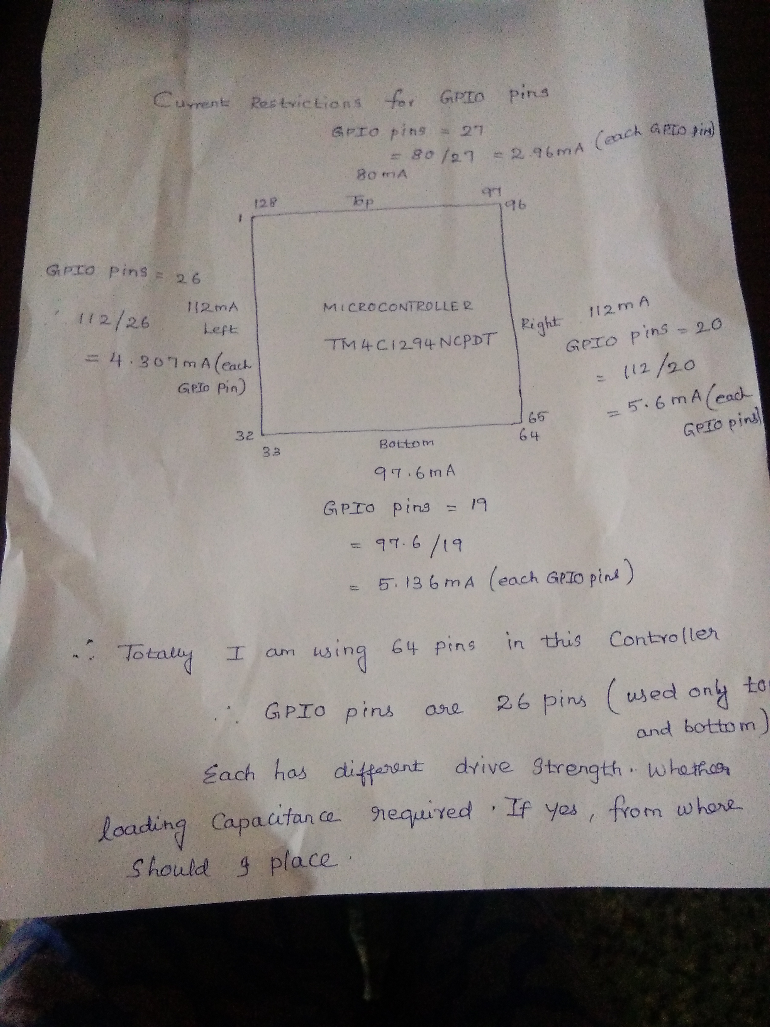
I am going to design a power circuit to my board. I have gone through the data sheet about current restriction. They specifically mentioned for each side of cumulative current for GPIO pins. In TM4C1294NCPDT datasheet,  page no. 1822 mentioned about the I/O reliability and page no. 1823 mention the load condition for the GPIO pin. I couldn't understand, for which pin i need to add the capacitive loading.  

  • Hi Nishitha,
    page 1823 specifies the load conditions used on the various pins for all the timing measurements published in the datasheet. For example, if you go to page 1849, the timing measurements of the GPIO pins at different drive strengths are based on 50pF load which is mentioned in 1823. The capacitive loading is the amount of load you will be placing on the pin from your external device. If you limit the load to within the limit that is specified then the I/O reliability can be guaranteed for the specified duration and operating temperature range.
  • Hi Sir,
    I have gone through that pages, still i have little bit doubt . Can you please explain this scenario. If i am choosing RGB LED is connected to PN0 pin means how much current will source in this pin???
  • Hi,
    That will depend on how much load you place on the PN0 pin. The GPIO pin is configurable for different drive strength, i.e. 2mA, 4mA and etc. The drive strength means that the I/O is capable of sourcing the specified amount of current (i.e. 2mA) and still maintain the specified Voh/Vol in the datasheet. I don't think it will source much current if you are connecting to the base of the transistor in the RGB LED.
  • Hi Sir

    Thanks for your information.I have a doubt,  I am enclosing the picture whether i am calculated current consumption is right or wrong. I have referred TM4C1294NCPDT datasheet page no.1821 & 1822. Kindly help me from where this capacitive load value 50pf to be place.

    I have another doubt, i have calculated the current consumption for micro controller based on page no 1880. I have calculated only Irun, Isleep, I deepsleep for 120Mhz at 85 degree Celsius for condition only Vdd,Vdda and peripherals=all ON including MAC and  PHY whether it is right or wrong?? I am going right path....

    Please clarify it...

    Sorry for the inconvenience

  • Hi,
    The 50pF loading mentioned in the datasheet means that the assumptions about the I/O reliability is based on using a 50pF load. It is not that the datasheet is asking you to place 50pF load on every GPIO pin. As I mentioned, the amount of load on each pin depends on the device you place on the pin. It may be smaller than 50pF. You need to check the datasheet of your external device.

    Also note that in table 27-9 the GPIO current restriction data is based on design simulations, not tested in production. Can you voltage regulator supply the required amount of current?

    Please also refer to the TM4C123 system design guideline on the GPIO section in page 41.

    www.ti.com/.../spma059.pdf