This thread has been locked.

If you have a related question, please click the "Ask a related question" button in the top right corner. The newly created question will be automatically linked to this question.

TM4C1294KCPDT: ADC sample hold Rs values for single ended ANIx inputs

Guru 55913 points
Part Number: TM4C1294KCPDT
Other Parts Discussed in Thread: TIDA-00778, INA240,

Does ANIx differential Rs input note (i) in ADC electrical specification and tables 15-4/5 maximum Rs values remain relative for single ended inputs? Note (i) states (differential input) then Rs values are a multiple of NSH cycles for single ended ANIx inputs, especially at sample rates of 2MSPS versus 1MSPS?

Otherwise it seems the maximum Rs series resistance value in single ended mode as depicted in figure 15-7 is not the end result @2MSPS? The TSHn encoding values for single ended ANIx inputs seem to reflect the source resistance times NSH cycles and not exactly the Rs values shown table 15-4/5. For example with hardware averaging 2x @2MSPS sequencers; figure 15-4/5 Rs/FCONV values seem to make no sense and Rs 500 is more like 8x the maximum listed, so a TSNh 2x encoding produces (Rs500 * NSH-8) = 4kRs and a reduced sample rate.

So it seems Rs resistance values are only a place to begin factoring ANIx input resistance relative to our ADC configuration and not the end result in all cases?  Wiki and TI ADC seminar SAR documents do not provide any details in this area.

Table 15-3 notes:

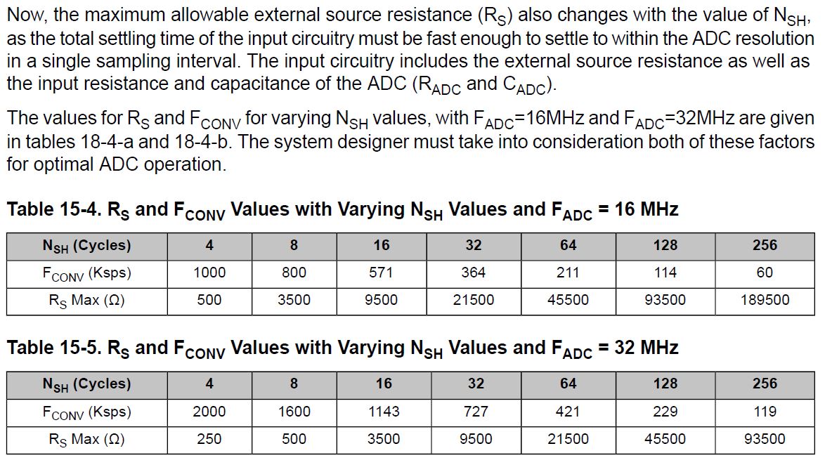
Now, the maximum allowable external source resistance (RS) also changes with the value of NSH,
as the total settling time of the input circuitry must be fast enough to settle to within the ADC resolution
in a single sampling interval. The input circuitry includes the external source resistance as well as
the input resistance and capacitance of the ADC (RADC and CADC).

  • Hi BP101,

     I'm not clear with your question. I tend to think these Rs values in the table are based on Spice simulation with extra margin built into it. I don't think the Rs is a linear equation wrt Nsh. Based on the table, @2MPS the Rs is not exactly half of what it is @1MPS for a given Nsh for which is only true with Nsh=4. I can only say the table serves as guide for system design for consideration of the maximum Rs to ensure proper input settling time. If your question is why the Rs is 500 at Nsh=4 or any values as listed in the table then I don't have an answer for it. 

  • Hi Charles,

    I think you missed the point that note (i) specifies Rs values are for Differential inputs and leaves out single ended inputs. Might note (i) suggest the tables are only valid for differential inputs? A single ended input Rs would be relative to ground specifically drawn as a value Rs in a resistive divider not as a series impedance.

    Perhaps the note (i) is misleading and the figure 15-7 is not being properly drawn to depict Rs as resistance relative to ground, since +Vs is not depicted relative to either table 15-4/5.

    Perhaps the +Vs side has Rs is drawn in the wrong location thus validates both tables as being series source (impedance) and not series resistance to ground?

    Hence the confusion to properly relate either tables values relative to a voltage divider where one side of Rs is always tied to ground for single ended ANIx inputs. 

    Why is note (i) being stated as differential and single ended input left out as there is no differential with single ended inputs? 

    How does hardware oversampling effect the NSH cycles in the Rs maximum resistance indicated being less or more than either table 15-4/5 indicate? Seems there would be double the ADC clock NSH cycles say @2x oversampling thereby doubling the maximum Rs values in either table?

  • Hi BP101,

     Can you please tell me which note (i) you are referring to?

    I see two of them in the ADC electrical section.

      The above footnote (i) is related to the these parameters.

    The above footnote (i) is related to the below parameter which is related to the input common mode voltage, nothing about the Rs value in differential mode as far as I can tell. 

  • What are you trying to say here? BTW: Quote is broken IE 11 browser highlighting a statement only bounces up when we click on Quote. Post button is also doing odd things this week.

    Rs = Analog source resistanc (i) being defined as the average of differential inputs. That note defines single ended ANIx inputs as being exempt from the effects of Rs, besides what hardware oversampling may add or subtract from Rs relative to NSH cycles. Seemingly Rs only relates to average of (differential inputs) where 2 ANIx channels are being configured to sample an analog signal.

    The reason to ask is ADC sequencer is randomly locked up by flyback spikes from monitoring bus voltage via an resistor divider, 9.1k to ground is not in series with signal as Fig. 15-7 shows. Otherwise we have 1.53 Megohms of series resistance from voltage source going into ANIx channel. So Rs values can't be in series with ANIx input and NSH table values to make any since for single ended inputs. Now we had to recently change ANIx input decoupling cap from 0.1uf to 100pf when the lockups of only ADC0 SS0 started to occur. Setting the NSH encoded value to reflect Rs= 9.1k has made the sequencer lockups more frequent.

    What is the proper NSH value to set for 1.5 Megohm series resistance into single ended ANIx channel as Rs is being defined by note (i)? Datasheet is not defining how Rs even relates to single ended or 1 and only 1 ANIx input. It seems to me they meant to suggest Rs table values are relative to ground in a branch divider and should not have been depicted as a series resistance in Fig.15-7.  

  • Hi BP101,

    BP101 said:
    Rs = Analog source resistanc (i) being defined as the average of differential inputs. That note defines single ended ANIx inputs as being exempt from the effects of Rs,

      To me, the Table 27-45. ADC Electrical Characteristics for ADC at 2 Msps only means the parameters listed are pertaining to 2Msps. It didn't say the table is only meant for differential inputs and not single-ended inputs except for the parameter VINcm (common mode voltage, differential mode) where the note (i) is applied. The only Rs that is mentioned in this table is the 250ohm which is the max resistance which corresponds to Nsh=4 according to Table 15-5 with Fadc=32MHz. 

      To avoid noise coupling to the AINx, I think you want to make sure you have quite digital signals adjacent to the AINx. Other analog signals adjacent to the AINs should have the same source resistance. 

      In the system design guideline app note, it is suggested that If resistor dividers are used to scale an input voltage, then best results can be achieved with low-value resistors. The resistor from the ADC input to ground should ideally be less than 1 kΩ. Avoid values higher than 10 kΩ unless a large filter capacitor is present. Your resistor divider has 9.1k currently. 

        The datasheet does not have Nsh for 1.5Mohm Rs. The max number of Nsh is 256 for which the Rs is about <200k. I think you goal should be to reduce the settling time, not to increase it. I think the below equation may help.

     ( Cext + Cadc) x ( 1 - 1 / (2 ^ (12 + 2)) = Cext where the 12 comes from 12bit ADC and the extra 2 means to allow the Cext to recover to 1/4 LSB and Cadc=10pf from the datasheet. Solving for Cext = 16383 x  10pf = 163.8nF. Currently you have 100nF. Can you try changing to >163.8nF and see it makes a difference?


  • >> It didn't say the table is only meant for differential inputs and not single-ended inputs except for the parameter VINcm (common mode voltage, differential mode) where the note (i) is applied.

    I realize it did say this but since Rs does indeed have note(I) it is implied to be differential by default since it leaves out any mention of a single ended connection. If Rs values are also meant for single ended ANIx inputs the note should include that fact or leave out note (i) entirely on any single table entry or FIg 15-7. None of it makes any logical sense to how a circuit would input into the ANIx input.

    >>The datasheet does not have Nsh for 1.5Mohm Rs.

    That is why I don't believe Rs is series resistance shown in Pspice model and Fig 15-7 is not drawn correctly to indicate Rs is indeed connected to ground, not in series with the ANIx input signal as it has been depicted.

    >> The resistor from the ADC input to ground should ideally be less than 1 kΩ. Avoid values higher than 10 kΩ unless a large filter capacitor is present. Your resistor divider has 9.1k currently.

    Yet most every TI evaluation kit (RDK) uses 9.01k to ground and past 6.8k choice value for LM3S SAR ADC. In our case refer to TIDA-00778 (schematic) though F286x MCU the SAR ADC should be same as TM4C employs. Agree the Rs 9.1k value +2.5k puts NSH value (11.6k) above table values. Something to consider, reduce Rs below NSH will reduce settling time too by using smaller values caps. A problem with lowering ANIx signal sample threshold closer to ground (1k/75mv) is undershoot spikes may cause sequencers latch up and ground noise is also sampled. Hence we often see TI engineers use Schottky diodes tied to 3v3, anode on ANIx to pull undershooting signals above ground. That didn't seem to help stop random latch up from occurring even when anode was tied to ground.

    >> Currently you have 100nF. Can you try changing to >163.8nF and see it makes a difference?

    Currently 0.1nf but ADC counts still go very high when PWM pulses appears on the DC bus, no avoiding that last symptom. And 200pf makes counts follow PWM wave produce current like wave shape in ANIx dividers even @24vdc. So the 0.1nf stopped low voltage PWM from producing high voltage samples (85v) peaks 24vdc. Fact is the 100nf made things worse required reducing sample settling time so it don't clump PWM pulses as wave shape. We past noticed same with EK-XL with ANIx series R 940k and 6.8k Rs to ground plus multiple ferrites and never figured the 100nf (.1uf) was causing voltage divider to become a high pass filter. So we must need low pass filter only to stop PWM pluses from being sampled. They are not true DC and very narrow spikes above input supply rail.
  • >> To avoid noise coupling to the AINx, I think you want to make sure you have quite digital signals adjacent to the AINx. Other analog signals adjacent to the AINs should have the same source resistance.

    That may be a problem since one INA240 input has no Rs tied to ground and DC bus voltage ANI-8 pin 124 exists between two analog comparator C2- input temperature sensors 500R outputs 200n near ANI-7,9 MCU pins 123,125. The only time ADC sequencer locks my occur during rough motor starting. A FOC startup crash can produces HV spikes above supply rail or when 24vdc supply crow bar may pulse several times to reduce current, ticks several times.

    Oddly making ANI-8 pin 124 input for ADC0 SS0 TNSH 0x66666666 (Rs=9.5k Max) can lock SS0 during PWM pre-charge time. Oddly SS0 TNSH 0x44444444 (Rs=3.5k Max) works more often without locking SS0 if pre-charge is set 10ms or less.

  • Hi Charles,

    Tina analysis results are in and Rs seems to be relative to ground not the source signal. Judging from actual live results; tables 15-4/5 are only showing external Rs value, not adding the internal Radc (2.5k) to each entry. The text above the tables would lead most readers to think Radc was already added.

    Seemingly 2x hardware averaging (HWA) though not stated doubles the Rs max allowed. Since the NSH hold time is doubled too as a result, that seems plausible. Attached are the Tina results and 200n with Rs 4.87k (Result 15) seems best, yet earlier testing with 0.33uf up to 10uf did not produce useable results. Seemingly  Rs 4.87k has stopped SS0 lockups 100pf to ground, 0x4 encoding. Perhaps Rs+Radc = 7370 ohms * 2xHWA = 14,740 ohms maximum allowable TSHN 0x4 encoding?

  • Also installed a OnSemi 3v3 TVS on DC Bus voltage ANI-8 parallel to Rs, when changing 9.1k to 4.87k. Same time installed TVS to 3 other shared SS0 ANIx inputs. The OnSemi 3v3 TVS are gull eared easier to mount and react in 1ns to transients above 3.6v.
  • Hi BP101,
    I find this app note about calculating Rs and Cext to use on the ADC pin which I hope will help. Even though it is not an app note specific for TM4C129 but the concept is much the same.
    www.ti.com/.../spna118b.pdf
  • Hi Charles,

    So the TM4C1294KCPDT -NCPDT datasheet incorrectly suggest Rs is resistance but in fact is source impedance, they are not the same things. That makes more sense with frequency as the series source impedance changes relative to the input frequency at ANIx inputs. Several places in the datasheet claim Rs is resistance when it should be stated as impedance.

    That explains why the TSHN encodes seem to revolve around the network divider ground resistor when the source series resistance is well above the maximum allowed Rs impedance in either table.

  • Hi BP101,
    The source impedance is the equivalent Zs when looking out by the ADC. The Rs is just part of the Zs calculation which is also dependent on the passive Cext and frequency of the input.
  • Read that now in the design guide Rs is part of Zs impedance. Yet the Rs in reality is not only reflecting signal source impedance rather more so the divider network. If that were not true high values of ground resistors would not randomly lock up the sequencer when sample count suddenly spikes up near 4096. Not even sure if Tina can determine what the input dividers impedance is relative to ANix input frequency or how it might change Rs values.

    BTW:
    Something is still wrong with the posting frame buttons, we now have to refresh the page every time just to click on reply or edit. What ever was recently done is now making IE 11 web pages difficult to navigate.
  • BTW: Design guide last note does infer HWA increases the charge on Cadc and produces a higher input impedance Zs.

    Realistically it seems 2x HWA doubles each Rs table value relative to ADC clock rate and NSH hold times when Cs must be kept low 0.1n-0.2n and Zs is very high 800k - 2megohms. We tested Cs 47n, Rs 5k, produced to much roll off to EMF zero crossing sinusoidal signal making it more saw tooth shaped.
  • Reading Tina help the transient Analysis can show impedance (Zs = Rs) if we add an Ohm meter on the ANIx input of the voltage divider.

    So the series impedance (Zs) for 1.5Megohms (Rs) with 4.87k to ground, our Zs = 9.86k impedance. TM4C129x Design guide confirms NSH hold times double the table Rs values via (2x HWA), ADC0 2MSPS table then starts @500 ohms impedance with TSHn=4 or (0x0) encoding.