


Part Number: EK-TM4C123GXL
Hi,
I already have a working interrupt driven SSI to communicate with my Winbond flash and recently I have dived into the realm of DMA. I thought it would be great to incorporate it with my Winbond code to make data transfer faster and to reduce CPU load. Has anyone done it before? I can't seem to find anything about this in the forum.
Currently, I have created an spi_transfer function which, when called, will setup and transfer the command / address bytes first. Then after the DMA transfer has completed, the SSI ISR will be triggered. Once triggered, the ISR will setup another DMA transfer in order to write / read data bytes that we are interested in.
For example, if I want to read the device id and manufacturer id of the winbond flash. The flash requires the master to send WB_READ_ID followed by 3 bytes of 0x00, then the flash will spit out the device id + manufacturer id. Below is a diagram to illustrate the transfer:
XX = don't care
// Transmitting 4 data bytes and expects two bytes of device id + manufacturer id
TX RX
WB_READ_ID XX ----
0x00 XX |______ Transferred during the first DMA transfer
0x00 XX |
0x00 XX ----
// Master needs to drive clock to allow man_id and dev_id to be shifted out
0x00 man_id ----_____ Transferred during the second DMA transfer
0x00 dev_id __|
My code is as follows:
// Initiate transfer by transferring cmd / addr bytes first
//*****************************************************************************
//
// Initiate communication with flash by transferring command / address bytes
//
//*****************************************************************************
void ssi_transfer(uint8_t *cmd_buf, uint32_t cmd_count, uint8_t *tx_buf,
                  uint32_t tx_count, uint8_t *rx_buf, uint32_t rx_count) {

    g_ui8SSITxBuf = tx_buf;
    g_ui8SSIRxBuf = rx_buf;

    g_ui32SSITxCount = tx_count;
    g_ui32SSIRxCount = rx_count;

    //
    // Enable the uDMA interface for both TX and RX channels.
    //
    SSIDMAEnable(SSI0_BASE, SSI_DMA_RX | SSI_DMA_TX);

    //*************************************************************************
    //uDMA SSI0 RX
    //*************************************************************************

    //
    // Put the attributes in a known state for the uDMA SSI0RX channel.  These
    // should already be disabled by default.
    //
    uDMAChannelAttributeDisable(UDMA_CHANNEL_SSI0RX,
                                UDMA_ATTR_USEBURST |
                                UDMA_ATTR_ALTSELECT |
                                (UDMA_ATTR_HIGH_PRIORITY | UDMA_ATTR_REQMASK));

    //
    // Configure the control parameters for the primary control structure for
    // the SSIORX channel.
    //
    uDMAChannelControlSet(UDMA_CHANNEL_SSI0RX | UDMA_PRI_SELECT,
                          UDMA_SIZE_8 | UDMA_SRC_INC_NONE |
                          UDMA_DST_INC_8 | UDMA_ARB_4);
    //
    // Set up the transfer parameters for the SSI0RX Channel
    //
    uDMAChannelTransferSet(UDMA_CHANNEL_SSI0RX | UDMA_PRI_SELECT,
                           UDMA_MODE_BASIC,
                           (void *)(SSI0_BASE + SSI_O_DR),
                           cmd_buf,
                           cmd_count);


    //*************************************************************************
    //uDMA SSI0 TX
    //*************************************************************************

    //
    // Put the attributes in a known state for the uDMA SSI0TX channel.  These
    // should already be disabled by default.
    //
    uDMAChannelAttributeDisable(UDMA_CHANNEL_SSI0TX,
                                UDMA_ATTR_ALTSELECT |
                                UDMA_ATTR_HIGH_PRIORITY |
                                UDMA_ATTR_REQMASK);

    //
    // Configure the control parameters for the SSI0 TX.
    //
    uDMAChannelControlSet(UDMA_CHANNEL_SSI0TX | UDMA_PRI_SELECT,
                          UDMA_SIZE_8 | UDMA_SRC_INC_8 |
                          UDMA_DST_INC_NONE | UDMA_ARB_4);


    //
    // Set up the transfer parameters for the uDMA SSI0 TX channel.  This will
    // configure the transfer source and destination and the transfer size.
    // Basic mode is used because the peripheral is making the uDMA transfer
    // request.  The source is the TX buffer and the destination is the SSI0
    // data register.
    //
    uDMAChannelTransferSet(UDMA_CHANNEL_SSI0TX | UDMA_PRI_SELECT,
                           UDMA_MODE_BASIC,
                           cmd_buf,
                           (void *)(SSI0_BASE + SSI_O_DR),
                           cmd_count);

    // Begin sending command / address bytes and pop out return bytes
    chip_select(~GPIO_PIN_3);

    //
    // Now both the uDMA SSI0 TX and RX channels are primed to start a
    // transfer.  As soon as the channels are enabled, the peripheral will
    // issue a transfer request and the data transfers will begin.
    //
    uDMAChannelEnable(UDMA_CHANNEL_SSI0RX);
    uDMAChannelEnable(UDMA_CHANNEL_SSI0TX);

    //
    // Enable the SSI0 DMA TX/RX interrupts.
    // Do I need to include SSI_DMATX as well?
    //
    SSIIntEnable(SSI0_BASE, SSI_DMARX);

    // Wait until the SSI chip select de-asserts, indicating the end of the
    // transfer.
    while (!(GPIOPinRead(GPIO_PORTA_BASE, GPIO_PIN_3) & GPIO_PIN_3));
}
// ISR
void SSI0IntHandler(void) {
    GPIOPinWrite(GPIO_PORTB_BASE, GPIO_PIN_2, GPIO_PIN_2); // indicate ISR entry

    uint32_t ui32Status;
    uint32_t ui32Mode;

    ui32Status = SSIIntStatus(SSI0_BASE, 1);

    SSIIntClear(SSI0_BASE, ui32Status);

    if (g_cmd_sent) {
        chip_select(GPIO_PIN_3);

    } else {
        // Enters here meaning command / address bytes were sent
        // Setup another transfer for the data that we're interested

        g_cmd_sent = 1; // signal that cmd and addr were sent so next
                                        // ISR entry will pull SS line HIGH

        ui32Mode = uDMAChannelModeGet(UDMA_CHANNEL_SSI0RX | UDMA_PRI_SELECT);

        // RX DMA complete
        // If it's a write, g_rx_dst_inc will be UDMA_DST_INC_NONE
        // if read, g_rx_dst_inc = UDMA_DST_INC_8
        if (ui32Mode == UDMA_MODE_STOP) {

            uDMAChannelControlSet(UDMA_CHANNEL_SSI0RX | UDMA_PRI_SELECT,
                                  UDMA_SIZE_8 | UDMA_SRC_INC_NONE |
                                  g_rx_dst_inc | UDMA_ARB_4);

            uDMAChannelTransferSet(UDMA_CHANNEL_SSI0RX | UDMA_PRI_SELECT,
                                   UDMA_MODE_BASIC,
                                   (void *)(SSI0_BASE + SSI_O_DR),
                                   g_ui8SSIRxBuf,
                                   g_ui32SSIRxCount);

            uDMAChannelEnable(UDMA_CHANNEL_SSI0RX);
        }

        // TX DMA complete
        // If it's a write, g_tx_dst_inc will be UDMA_SRC_INC_8
        // if read, g_tx_src_inc = UDMA_SRC_INC_NONE
        if (!uDMAChannelIsEnabled(UDMA_CHANNEL_SSI0TX)) {
            uDMAChannelControlSet(UDMA_CHANNEL_SSI0TX | UDMA_PRI_SELECT,
                                  UDMA_SIZE_8 | g_tx_src_inc |
                                  UDMA_DST_INC_NONE | UDMA_ARB_4);

            uDMAChannelTransferSet(UDMA_CHANNEL_SSI0TX | UDMA_PRI_SELECT,
                                   UDMA_MODE_BASIC,
                                   g_ui8SSITxBuf,
                                   (void *)(SSI0_BASE + SSI_O_DR),
                                   g_ui32SSITxCount);

            uDMAChannelEnable(UDMA_CHANNEL_SSI0TX);
        }
    }

    GPIOPinWrite(GPIO_PORTB_BASE, GPIO_PIN_2, ~GPIO_PIN_2); // indicate ISR exit
}
So my problem is, when I step debug the program, I will get the correct man_id and dev_id (0xef and 0x17) but when I do a full run, the IDs are wrong (0x90, 0xff). Here is a screenshot of the full run on the logic analyzer:
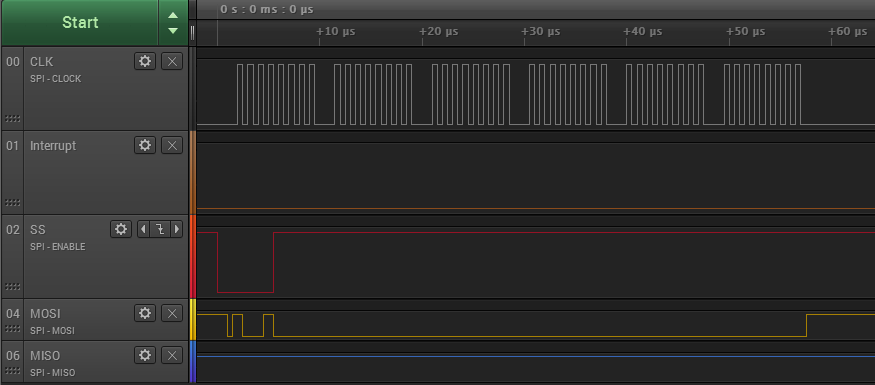
As shown in the screenshot, the SS line is pulled HIGH too soon and I am not sure why.
Just to make sure my DMA is working properly, I have also tried to transfer all the data in one DMA transfer instead of two (as described earlier) which gives me the correct result as shown in the screenshot below:

Is there something that I am missing or not understanding correctly about uDMA?
Best Regards and Thanks in Advance
Jacky

