This thread has been locked.

If you have a related question, please click the "Ask a related question" button in the top right corner. The newly created question will be automatically linked to this question.

EK-TM4C1294XL: Understanding ADC timing in TM4C

Part Number: EK-TM4C1294XL
Other Parts Discussed in Thread: LM3S8971, LM94022, INA240

Hi everybody, 

I write because I don't find a correlation between the theoretical and the measured timing of the ADC in TM4C1294.

TIMER0 triggers the ADC0 at 5 kHz. The ADC0 is configured to sample 8 channels: 2 on ADC0SS0, 2 on ADC0SS1 and 4 on ADC0SS2. INT_ADC0SS2 generates an interrupt. 

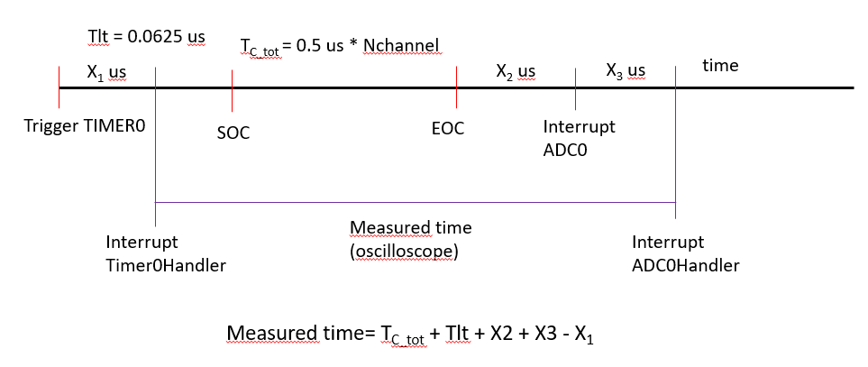
The same TIMER0 generates also an interrupt. I use it to measure the time between the trigger and the end of conversion. 

The ADCclock is configured to run at 32 MHz. It has been configured with the following instruction:

ADCClockConfigSet(ADC0_BASE, ADC_CLOCK_SRC_PLL | ADC_CLOCK_RATE_FULL, 15);

So, I expect a theoretical conversion time of:

Tconv=1/(ADCclk/(12+4))= 0.5 us /sample (it's not a coincidence that 2 Msps is the maximum throughput of the ADC) 

so, for 8 samples the total time should be  Tconv*Nsamples=4 us.

However, I measure about 9 us between the trigger and the ADC interrupt. 

Besides, if I use a hardware oversample of 16x, I expect to have:

 Tconv*Nsamples*foversample=0.5*8*16=64 us.

However, the measurement shows about 33 us.

So, my question is why the conversion time is different in both conditions in different ways? 

Thank you for your time,

Regards

  • Hi Michele,

    Seems you did not add the latency (2*ADCLKS or 62.5ns @32Mhz) and Tc= 0.5us @2MSPS includes (Ts=125ns).

    Depending on your TSNH encoded hold time set for the FIFO step the sample time will increase when hardware averaging (x16) thus divides 2MSPS per datasheet tables. Yet Tc should not increase according to the datasheet ADC electrical specifications. Had that same discussion past with another helper in this forum. It would seem Tc may be a factor of hardware averaging omitted from datasheet.

    If that is true perhaps it would be 16 * Tc500ns = 8us total Tc window factored by 2MSPS/16 + TSHN.
  • Hi Michele,

    On paper your calculation is correct but I don't know how you implement such measurements in your application. There are several factors you need to take into consideration.

    1. First you break the 8 channels into 3 different sequencers. The ADC state machine will take some cycles to switch from one sequencer to another.

    2 When the ADC finishes the conversion, it generates the interrupt. It takes some cycles to enter its ISR. In the ADC ISR you probably try to take the difference between the Timer register (GPTMTnR) and the timer free running counter (GPTMTnV). I hope this is how you take the measurement. You need to subtract the time that is due to the interrupt latency time taken by the CPU to enter the ISR (the CPU needs to save its context onto the stack).

    3. There are other minor factors that are intrinsic to the design implementation. For example, when the timer generates a trigger signal to the ADC. To avoid long timing path, the signal is normally piped through flops. On the receiving end of the ADC, it is again piped (registered) to break the timing path. Same thing is done when the ADC asserts it interrupt request signal to the NVIC. Even though these latency cycles are small they are nevertheless needed for consideration.

    For your experimental purpose, try to use all 8 channels on SS0. I think you should see some improvements.
  • BTW: Specification says TLt = 0.5us "latency from trigger to conversion" but think it should say start of sample, not conversion. As that would seemingly add 16* 500ns = TLt8us or 500ns into each oversample in the circular FIFO averaging. Your 5Khz GPTM ADC trigger (200ms) should never overrun the FIFO sampling frame.
  • Thank you for your reply.


    Actually, I am considering Nsh = 4 ADC clock cycles.

    Even if I consider the latency I am far from the measured value. Probably I am missing something. And I am worried mostly for the differences that there are when I use hardware averaging (Tc/sample is reduced when I use hardware averaging).
  • Both posters - to my mind - provided valuable insight.

    Yet Vendor's Charles, 'Stole my Thunder' - that being your 'INTERMIX' of 3 different ADC Sequences!      Does that not enforce 'UNWANTED & UNKNOWN VARIABILITY' - INTO YOUR MEASUREMENT?

    As Charles stated, I questioned the 'precision & repeatability' of the 'Timer Trigger.'      Yet poster BP - has 'dived deep' (we APPLAUD - love to see MORE!) and presented a 'published spec!'    (ALWAYS ... Good That!      Beats the hell out of naked opinion... (too often the 'norm')

    To achieve the 'purest, most logically correct measure'   would not your confining such experiment to ONE SINGLE ADC Sequence - involving all 8 (max) ADC conversions - prove by far - best?

    Unknown (to me) is the 'response time' of the ADC's interrupt generation (which is said) to occur 'post the completion' of the conversion.    (that's 'vague' is it not?)    But unless BP can dig further - remains uncertain/unknown.

    And one last gasp - (unlikely in your case - but valid for 'Generalizing such Findings' (how 'some' get the BIG Bucks!) - the presence of other (possibly competing)  program code - running while you perform such measures (especially if that 'other' is 'higher priority') may, 'Push certain of your 'measures' (somewhat towards) the  back of the bus...   (and that's 'my'  - usual seated position... Do - introduce yourself)

  •    

    Thank you for your reply, Charles.

    I am measuring the time with the oscilloscope (changing the state of a GPIO).

    I am aware of the differences between the conversion time and the way I use to measure the time (I am not considering X1, X2 and X3 in the timing diagram). However, I think that differences are too high.

    I have followed your suggestion to use only a sequence, but I have noticed only a slight decrease in the measured time (about 0.15 us).

    The trouble is that:

    - without hardware oversampling 

    Tmeasured=1.1 us/sample (with all delays)  

    Ttheoretical=Tc + Tlt = 0.5 us/sample + 0.0625 us

    - with hardware oversampling 16x

    Tmeasured=4.125 us/sample (with all delays)  

    Ttheoretical=Tc * 16 + Tlt = 8 us/sample + 0.0625 us

    So, I am not considering some delays in Ttheoretical without oversampling. However, these delays seem to disappear when I use oversampling, because the measured time is much lower than the theoretical one.

    Thank you again for your support. 

  • Hi Michele,
    I don't have a good answer yet. Can you please try a few things?

    1. Can you take measurements for 1 channel only and 4 channels? This way we can confirm that the conversion time is linear.
    2. Are you setting the GPIO pin in the timer interrupt and clearing the pin in the ADC interrupt? This should be a fine way but can you try to use two different GPIO pins? Both pins will set respectively in the Timer and ADC interrupt ISRs. Take the difference between them. I just wanted to rule out you are measuring the time from the ADC interrupt to the Timer interrupt.
    3. In your ISR to clear or set the pin can you do DRM (direct register modification) to the Data register instead of calling GPIOPinWrite(). This may save a bit of cycles even though not much. Perhaps one thing to ask is how are you clearing the pin in your code. If you perform some type of toggle that requires read-modify-write then it can take more cycles to execute.
    4. What is code compiler optimization level?
    5. As asked by cb1, do you have any other interrupts other than the Timer0 and ADC? Please note that higher priority interrupt can preempt the ADC.
  • Greetings Charles,

    I (am) trying to exit this 'LIKE-less'  forum - yet  this - and the other (related thread)  'VCO @ 480MHz  (potentially)  able to generate SysClk @ 120MHz AND ADCClk @ 32MHz' - has 'briefly' - sucked me in.

    https://e2e.ti.com/support/microcontrollers/tiva_arm/f/908/t/706611

    Our poster here believes that he's achieved 32MHz as his ADC Clock - yet has he (really) tested & verified?

    As firm/I engage w/multiple ARM MCUs - across many vendors - we too have met the requirement - to 'REALLY MEASURE the ADC's Conversion Rate!'     And - the 'toggle of GPIO' - has NOT met the advanced requirements - of our 'serious' clients.

    A method (which firm/I - believe substantially  (pardon) BETTER) would see the,  'Introduction of a precise, rising, linear voltage ramp - injected into a, 'SINGLE ADC Channel' - with that Channel 'Commanded to perform' - an eight sequence ADC Conversion!     As the 'slope' of this precision, linear voltage is known - the 'Actual MOMENT in TIME' - when EACH CONVERSION (REALLY OCCURRED) - CAN  (FAR MORE) PRECISELY - BE DETERMINED!     (i.e. Each/Every of the 'compromised & indirect (lesser) alternative measures'  (interrupt driven GPIO) have been eliminated!)

    Such a Linear Voltage Ramp must be able to drive from (near) 0 Volts to (near) 3V3 (or Max ADC V_in) w/in the 'suspected time duration required' of,  'ALL EIGHT ADC CONVERSIONS!'     And do so - while fully complying w/each/every of the ADC's Input specifications.   Our use of past, proven analog designs - AND new,  ARM Cortex M7s (equipped w/hi-speed DAC)  speeds & eases - such (highly useful)  Linear Voltage Ramp Creation & Application!

    Such Advantaged,  'Direct MEASUREMENTS' - most always - trump those 'compromised, indirect (lesser) methods.'      Even though those  'compromised methods' prove easier - especially  as those  'compromised methods' prove easier!       (One may properly ask - is the objective 'EASE' ...  or 'REAL (and valid) RESULTS?')

  • Hi cb1,

      That is an excellent suggestion to check if the VCO is running at 480MHz. I will even suggest one more experiment for the poster to try. Configure the ADC clock to source from PIOSC (16MHz) instead of the PLL(480MHz/15=32MHz) and see what measurements she is getting. The PIOSC runs at 16MHz. If the measurements are the same between using PLL and PIOSC then it is next thing to investigate what went wrong. 

    Michele,

      Please post your entire code for review. 

  • My 'most recent' contributions (prior to departing this 'LIKE-less'  forum) aimed at two areas:

    • Can (both) SysClk @ 120MHz  AND  ADCClk @ 32MHz - be achieved - via the MCU's VCO running @ 480MHz?     (central issue - missed by ALL - is the 'validity of the Div. by 15' - which I strived to well detail.)
    • A proven superior method - to determine the 'Real World' (measured under LIVE Operating Conditions) Conversion Rate - of (any vendor's) MCU's ADC was also (herein) presented

    It's unclear if you are - w/in your (post above) - reacting to 'one or both' posted contributions.     Firm/I 'know these to succeed' - and have 'very profitably'  - Delivered/Sold both...

  • Hi Charles,

    I am not in laboratory in this moment. But I will reply with tests as soon as possible.

    In the meantime, I can reply with the past experience:

    1. I have already taken the measurements for different samples number and the time is linear. Tomorrow, I will came back to you with numerical values.

    2. Yes, exactly. Here, are you asking to add another pins and taking the difference between them?

    3. I am using GPIOPinWrite. I will switch to DRM.

    4. Level 3 - Global optimization

    5. Yes, I have other interrupts. However, ADC interrupt has the highest priority (0), Timer interrupt has priority 1.

  • Hi cb1_mobile,

    I am pretty sure the VCO is 480 MHz. However, I will check it to be sure.

    I am happy that you are sharing with us your knowledge in measuring the time of high/speed ADC. And actually, if you know that GPIO toggling is not a good method is because you have used it in the past.
    Anyway, when I will be able to have a setup with 'a precise, rising, linear voltage ramp' and without any kind of noise to have a so accurate measurement I will be happy to apply your method.
    The GPIO toggling obviously is not accurate because there are different CPU clocks to take in account between the events, but it is precise in the sense of measurement precision.

    However, my post here is not to measure time in a CERN-like environment, but to understand why there is discrepancy if I use hardware oversampling or not. So, maybe the ADCclk is not 32 MHz, but it would not be 32 MHz with or without oversampling.
  • The idea of PIOSC  is a good one! I will apply it to see if there are differences.

    However, what is not clear to me is the difference if I apply or not the oversampling. Because, without oversampling the ADCclk  seems running to 16 MHz, with 16x oversampling it seems running to 64 MHz (this is not possible obviously).

    I will let you know with the updates as soon as possible.

    The entire code is not possible, also because is a big project.

    I can show the instructions I use to set the CPU clock and ADC clock.

    ////////////////////////////////////////////////////////////////////////////////////////////////////////////////////////////////////////////////////////////

    uint32_t g_ui32SysClock;

    g_ui32SysClock = SysCtlClockFreqSet((SYSCTL_XTAL_25MHZ | SYSCTL_OSC_MAIN | SYSCTL_USE_PLL | SYSCTL_CFG_VCO_480), 120000000);
    
    //...
    
    SysCtlPeripheralEnable(SYSCTL_PERIPH_ADC0);
    
    ADCClockConfigSet(ADC0_BASE, ADC_CLOCK_SRC_PLL | ADC_CLOCK_RATE_FULL, 15);
    
    ADCHardwareOversampleConfigure(ADC0_BASE, 0x4);
    
    //...

    ////////////////////////////////////////////////////////////////////////////////////////////////////////////////////////////////////////////////////////////

    Thank you for your support.

    Michele

  • Hi Michele,

     I have collected some data myself. Please see below. With PIOSC as the source the average conversion time per channel is about 2.2uS. With VCO=480Mhz and divided by 15 for ADCCLK the per channel conversion is about 1.19uS. Yes, the 32MHz ADCLK does reduce the conversion time by about half compared to using PIOSC=16MHz. However, there is some hidden latency that eats up the overhead on top of the theoretical number. Let's see what you get when you have a chance tomorrow. 

    # of channels PIOSC (uS) Avg time/channel VCO/15 (uS) Avg time/channel
    5 11.2 2.24 6.25 1.25
    6 13.2 2.20 7.1 1.18
    7 15.3 2.19 8.3 1.19
    8 17.3 2.16 9.15 1.14
    Average   2.20   1.19
  • Here is additional data with oversampling. As you can see with 2x oversampling the per channel conversion time is the same as no oversampling while the 4x oversampling only double the conversion time per channel. This indicates that the design does not comply to the datasheet description. It looks like only the AVG[2:1] field in the ADCSAC register is taken and the AVG[0] is ignored. I will have an internal discussion for an errata update.


  • mm3010 said:
    Actually, I am considering Nsh = 4 ADC clock cycles

    That should produce FConv 2000Ksps (AKA-2MSPS).  Makes since when 4x oversample a single Tc @500ns period might decrease from division 2MSPS frequency of averaging periods but throughput is said to suffer. The acceleration you are reporting seems to makes since as a sample period is divided does it not become shorter but FIFO serial bit rate decreases in the same stroke. 

    Perhaps Tc value is derived indirectly from the circular FIFO rate in the ADC clock frame of each sequencer, not specifically the ADC clock speed alone.


  • mm3010 said:
    my post here is not to measure time in a CERN-like environment

    Thus - we share that objective.     Although many of our 'advanced' designs are sold to the Medical Device  AND  Defense community.

    Here's a quick/dirty summary - which argues in behalf of the superiority of the 'more precise' method - earlier proposed:

    • it is (properly) divorced from your MCU!       Many (serious) tech disciplines 'DISALLOW'  the 'DUT' - from (itself)  producing the 'confirming/verifying' measurement data.     (Rarely does the patient - lying  comatose -  'on the ER's table' -  direct the examination!)
    • it is MCU Agnostic - any vendor's MCU is 'Welcomed & Instantly Accommodated!'      Is it not (beyond) wasteful - to devise a test - suitable for  ONLY a Single MCU?
    • it avoids 'ALL Code-Writing Requirements' - simply run the MCU as normally operated - no (other) arcane MCU 'deep dives' required.   (Few succeed w/µDMA - on first go!)
    • it avoids the addition of  'extraneous code spurs' - which demand time & effort to create - and (may yet) - introduce (still further)  errors.
    • while I've 'Focused here - upon your specific 'Use-Case' - we developed such device to  properly,  'Speed, Ease & Enhance'  the 'Automated Testing' of MANY Analog Circuits' - even beyond the MCU's ADC (and Analog Comparators)

    Under NDA - we exhibited several versions of  this novel device - at  last month's 'Automatica' - in beautiful Munchen!     (multiple individuals & firms recognized & responded to our  'Value Proposition' - So Strong/Compelling/Recognizable - was its  impact!)       (Note that  'NONE/ZERO'  ... of those critical benefits - were  realized  by the,  'NONE too advanced, competing (cobbled) method!')

    The ability to devise (such effective) special devices & methods - which may be used repeatedly - across MANY  'Vendors, Applications & Disciplines - warrants your consideration.    (Should 'Real & Broadly REUSABLE -  ADVANTAGED METHODS' - as I believe - 'will' capture your interest.)   

    I believe the 'relative merit' of the two methods have been well compared/contrasted  ...  even with - and especially with - the 'diversion'  (perhaps) raised by, 'any kind of noise' & 'CERN-like.'    (such noise - if any - would  impact the succession of eight precision measurements (very) equally  (thus is 'effectively' cancelled out - is it not?)      (while likely wreaking 'far more havoc' - upon the 'relaxed, less restricted,  unspecified source' method...)

    There IS a CLEAR WINNER here!

  • May it be noted that while you've achieved (some) consistency of measurements - the actual, "Moment of TRUTH" (that point in time - in which the ADC actually/really - performs its conversion) - is unknown!     We may 'hope' that it occurs at a consistent & proportional rate - yet that has  - in NO WAY - been isolated & measured!

    Big Deal - except for the fact that several of our clients - reported unfortunate 'variation in such  conversion results' - when measuring - much as you (appear to have done so - here!     The likelihood of such 'VARIATIONS' grows quickly - as the code size expands - many interrupts are serviced - and not always - can the ADC be granted, 'Top Dog' and/or 'Interrupt Preemption!'     Thus the issue becomes much magnified - more impacting.

    And again - I don't believe that the 'Conversion has been (entirely) proved to have completed - via this method.'     Indeed an ADC Interrupt 'has' occurred - causing a 'GPIO marker' - but that does not - absolutely - advise nor inform - that the conversion has entirely completed!       (Data-Sheets are famed for - not always - making 'full & proper' claims.)      Your method  thus relies (heavily) upon 'hope' -  rooting for the data-sheet's accuracy.      Yet  is each claim indeed fact - and  is such fact  ALWAYS  Operational - and under ALL CONDITIONS!     Really?    (much hope/prayer - has entered the building...)

    Is that (really) SAFE?     User here has questioned the conversion rate for (some) reason.     In all cases but one - Ease & Quickness of Investigation -  has dominated (even replaced)  REAL & DIRECT MEASUREMENT!     Is that proper - and of greatest value - to user-clients?

  • Hi cb1,
    I want to clarify something. I do not use any interrupt. This is what I do for measurements.
    1. Set the pin high
    2. Trigger the ADC via the processor
    3. wait for the ADC interrupt flag to set
    4. Clear the pin
    5. Measure the width of the pulse.
  • Charles,

    I'm confused. (like that's unusual...)

    Please (better) detail:

    • 'Set the pin high' .... based upon what?
    • How do you detect the ADC Interrupt flag's being set? Via a looping Register Read, perhaps?      That's not detailed.
    • Why 'Clear the pin - and (only then) make the pulse width measurement?     Does not that 'clear effort' - consume time - adding ERROR?

    What do we REALLY KNOW about the 'sacredness' of the ADC Interrupt Flag?     Especially its ability to provide 'Precision and Always Repeatable Performance - under ALL Conditions!

    It is noted that  NONE of my previous '5 Key Points'  - detailing a (more) Serious Measurement Effort - have received comment.      Only the persistent defense of the 'One done from within the Device Under Test' - which proves  WELL OUTSIDE ACCEPTABLE PRACTICE!

  • Hi cb1,

     Prior to step 1, I have setup the ADC (i.e. the sequencer). It is just waiting for a trigger to start conversion. I didn't use timer as the trigger. I wanted to avoid the interrupt and have better control on when to start the conversion. I set a GPIO pin first and immediately initiate the sequencer by the processor (a software trigger) to start the conversion. I will poll until the interrupt flag is set and then clear the pin.

  • Hi Charles, 

    thank you for the results of your experiment. The different conversion time per channel (with or without oversampling) was the condition that caught my attention in the first moment. 

    I have repeated the measurement, without changing the GPIO status using DMR, so to compare my application with your results. And your results are comparable with mine. I report here only the results with 8 channels.

    # channels Oversampling Absolute time (mean) Std Dev Avg Time/channel
    8 4x 16.9 us 49 ns 2.11 us
    8 0 8.89 us 50 ns 1.11 us

    So, I have 0.05 us (2.16-2.11) less with 4x ovesampling and 0.03 us (1.14-1.11)  less without oversampling. But I think that this small difference is not due at the conversion time of the ADC, but it is due to the different setup. The most important result here is that the Avg time/channel decreases when the oversampling is enabled. For this reason, I think that I am missing something from the datasheet. 

    The delays we are discarding affect the measured time in the order of nanoseconds. 

  • Charles Tsai said:
    ... Sequencer - awaiting a trigger to start conversion - Timer-based trigger (replaced) by Processor trigger - avoids the interrupt and better controls the start of ADC conversion.

    Indeed that's (both) a resourceful and clever means of performing such, 'Conversion Duration Measure.'      

    While that method 'commands the MCU to your will'  - it does so 'outside' our poster's expressed intent!      (which was earlier noted as '5KHz,  Timer-based,  Conversion Trigger.')      

    Note too - multiple 'unknowns' invade - which are (likely) to prove, 'Program Sensitive' - thus difficult to readily detect and (potentially) distressing/degrading such 'Conversion Measure.'

    And - no 'Gauge of the accuracy' of such ADC Conversion 'Analog Values' are achieved - which IS of (some) importance - is that not so?

    The alternative, 'Monotonic, Precision Linear Voltage Ramp' - avoids (all) of these weaknesses - while presenting the MCU w/a properly matched impedance...     (again - not 'touched' - via the 'DUT does it all' method...)

  • mm3010 said:
    The delays we are discarding affect the measured time in the order of nanoseconds. 

    Might such a 'blanket statement' result  (more)  from 'hope' - while (avoiding) the potential impacts of  the MCU's Program - and the (sure) - 'challenging & competing demands'  of 'other' MCU Peripherals and program features?

    This 'ADC Conversion Rate' (must) have some importance to you (otherwise - what IS the point) and expecting ALL of the 'unknowns' to prove 'Non-Impacting' has NOT been well examined nor tested...

  • Hi Michele,
    I will get back with later. My bad that I had a mistake yesterday when I ran the PIOSC test. I had the ADC configured for half-rate conversion rate which doubles the conversion time. I also had some talks with my colleague about the PLL setting. Need some time to sort it out.
  • Hi Michele, cb1,

      I have taken some more data. You will need to bear with me here. Here is a short summary.

      1. I made a mistake in my earlier test for the PIOSC. I wrongly configured for half-data conversion rate. With the PIOSC as the clock source and running the ADC at full data rate I have average conversion time at about 1.25uS which is not too far from the 1Msps.

      2. When you configure for VCO=480MHz it DOES NOT give you 480MHz but rather only 240MHz. Due to some workaround implementation the SysCtlClockFreqSet() API actually configure the VCO for only 240MHz even though you specify for 480MHz. There is actually not a  SYSCTL_CFG_VCO_240 macro to use. Because the VCO is running at 240MHz, the ADCCLK after VCO/15 only gives you 16MHz. This is the reason you are getting close to 1Msps rather than 2Msps. 

      3.  If you configure for VCO=320MHz it DOES NOT really give you 320MHz but rather only 160MHz.  Because the VCO is running at 160MHz, the ADCCLK after VCO/10 only gives you 16MHz. This is the reason you will be getting about 1Msps if you choose VCO=320MHz and try to divide by 10 thinking you may get 32MHz on the ADCCLK.

      4. In order to get 2Msps, you will either choose SYSCTL_CFG_VCO_480 and divide it by 8 to get the ADCCLK=30MHz or choose SYSCTL_CFG_VCO_320 and divide it by 5 to get the ADCCLK=32Mhz. Please note that with SYSCTL_CFG_VCO_320 you will only get the SYSCLK=80MHz, not 120MHz. If you want to operate the device at the maximum frequency and wanting to obtain 2Msps on the ADC you will need to choose SYSCTL_CFG_VCO_480  and divide by 8 to get ADCCLK=30MHz. If you look at the result on cells I6 and K6 they are almost the same. The 32MHz ADCCLK does not significantly give you more throughput compared to running at 30MHz. The reason is that at 32MHz the SYSCLK=80Mhz so the CPU is running slower and all the latency that we talked about will be timed according to the slower SYSCLK.

  • HI Charles

    Charles Tsai said:
    . When you configure for VCO=480MHz it DOES NOT give you 480MHz but rather only 240MHz. Due to some workaround implementation the SysCtlClockFreqSet() API actually configure the VCO for only 240MHz even though you specify for 480MH

    It was explained by RTOS forum the main clock tree PLL block pre-divides the frequency by 2 but you now saying MainClockFrequencySet() has a bug? So we were only getting 8Mhz ADC clock div 30 in ADCClockConfigSet()?  How could that have so easily flown under the radar?  It seemed ADC clock was 2MSPS via div 15 (32Mhz) compared to 1MSPS of previous LM3S8971 MCU.

    Are you certain you are not overclocking the ADC module? 

  • Hi Charles,

    this sounds right compared to the results obtained with PIOSC.

    I will use SYSCTL_CFG_VCO_480 divided by 8 to obtain ADCCLK=30MHz. However, this is different from the example given in the Tivaware peripheral library user's guide, where it uses 480/24 to obtain ADCCLK=20MHz:

    //
    // Configure the ADC to use PLL at 480 MHz divided by 24 to get an ADC
    // clock of 20 MHz.
    //
    ADCClockConfigSet(ADC0_BASE, ADC_CLOCK_SRC_PLL | ADC_CLOCK_RATE_FULL, 24);


    Have you tried to apply the oversampling now?

    It seems that the ADCclk is faster than 30 MHz (it's like 60 MHz, that is 2 times the real ADCclk)!
    For example, with 4x oversample and 8 channels I am measuring 1.15 us avgTime/channel, that is much more than 2 Msps!

    Is this related to the SYSCTL_CFG_VCO_480 workaround?

    Thank you very much for the explanation of the workaround with SysCtlClockFreqSet().
  • Charles,

    None of this rather intense 'issue' - in any way - brought about by you.     Yet it (surely) GREATLY DISTURBS!

    And - we note - this issue WAS KNOWN - yet NEVER PUBLISHED/PROPAGATED - so high vendor cliffs - once more - claim new  victims!

    That 'failure to alert' appears an (unfortunate) yet (almost) 'grooved behavior' - does it not?
    And one NOT famed for - your Users', 'Care and Comfort!'

    Of perhaps even GREATER IMPORT/INTEREST ...  Does this 'just released' Tech Finding - impact ALL MEMBERS of the '129 family?     (that's of some import - is it not?)

  • Perhaps the main clock tree figure incorrectly shows ADC1/2 modules use same PLL output and PSYDIV divisor branch labeled as VCO output. That would certainly explain a few WTH is that PLL doing now head scratches..
  • Hi Michele,
    The example you see in the TivaWare peripheral library user's guide predates the workaround change that was implemented in the SysCtlClockFreqSet(). So the description is misleading. Needs to be updated.

    As far the oversample is concerned, I already explained it yesterday. I also measure 1.14uS with 4X sample rate. But in reality it is only oversampling at 2x instead of 4x. I mentioned yesterday that we will need an errata. It is more like below.

    What is written in the datasheet.
    AVG[2:0] = 0, no oversample
    AVG[2:0] = 1, 2x oversample
    AVG[2:0] = 1, 4x oversample
    AVG[2:0] = 1, 8x oversample
    AVG[2:0] = 1, 16x oversample
    AVG[2:0] = 1, 32x oversample
    AVG[2:0] = 1, 64x oversample

    [EDIT: 07/13/2018] Below were wrongly stated. See the latest post from me on July 13, 2018 9:35AM.

    In reality:
    AVG[2:0] = 0, no oversample
    AVG[2:0] = 1, no oversample
    AVG[2:0] = 1, 2x oversample
    AVG[2:0] = 1, 2x oversample
    AVG[2:0] = 1, 4x oversample
    AVG[2:0] = 1, 4x oversample
    AVG[2:0] = 1, 4x oversample

    AVG[0] is being ignored in the encoding.

  • BP101 said:
    So we were only getting 8Mhz ADC clock div 30 in ADCClockConfigSet()? 

    Yes, if you configure the VCO for 480Mh and after divide by 30 it is not 16MHz but rather 8Mhz. This is also new to me. Apparently, there was some issue with the clock generation logic where they need to create a workaround in the SysCtlClockFreqSet(). Perhaps the intention was to maintain compatibility and therefore, the SYSCTL_CFG_VCO_320 and SYSCTL_CFG_VCO_480 was still presented to the users but failed to realize that this impact the ADCCLK. My colleague is still digging up the history on this topic. 

  • Hi cb1,

    cb1_mobile said:

    And - we note - this issue WAS KNOWN - yet NEVER PUBLISHED/PROPAGATED - so high vendor cliffs - once more - claim new  victims!

    That 'failure to alert' appears an (unfortunate) yet (almost) 'grooved behavior' - does it not?
    And one NOT famed for - your Users', 'Care and Comfort!'

    Sorry, I do not agree with your statement that this is a known issue and is intentionally to be hidden. At least it is now known to three of us who are supporting the TM4C forum. With all that said, an errata is due urgently for clarification. 

  • Yet mm3010 reported the ADC sample clock is seems to be 60Mhz. So that claim was because of 4x oversample errata?

    What Tivaware version was the PLL/PSYDIV work around done?

    Odd thing about ADCHardwareOversampleConfigure() is if you put a hex divisor value (0x4) shown in REG text for pass value the call ignores the divisor.
  • Hi BP101,
    I think the problem is in the ADCHardwareOversampleConfigure(). Reading the source code I'm not sure why it is doing all the shifts when it can just write the argument into the register directly. I use DRM to write 0x1 (2x oversample) and 0x2 (4x oversample) and the conversion time looks to be correct in the sense that 0x1 is taking close to 2x amount of time to convert. With 0x3 it is taking 4x amount of time.
  • Hi Charles,

    I checked the call code via calculator and N << 4 is correct as it subtracts 1 from N passed in from the call for REG 66 value. But who know what the integer N does to the ADC modules clock as very little info in REG 66 text to explain how 0x70 relates to clock rate.

    We now see very nice ratio metric slope from INA240 sensors and LM94022 sensors seem very accurate. The oversampling 0x2 at 30Mhz ADC clock is great compared to 16Mhz, we were so fooled believe the Rs impedance @16Mhz.

    Thanks millions mm3010 for your persistence and Charles investigating ADC clocking conundrum!
  • Hi Charles,

    You were not trusting ADCHardwareOversampleConfigure() for loop shifting bits and it seems from quick calculator check it may have been doubling >> hex values in REG12.

    Perhaps it was done that way to pass decimal (1) in the call to make hexadecimal (0x2) and so on in REG12 bit field.


  • Hi BP101, Michele,

     I really apologize about the confusion. I think the code is trying to emulate the radical expression. For example, if user specifies 64x oversample as in ADCHardwareOversampleConfigure(ADC0_BASE, 64) then the radical of 64 is 6 to be written to the AVG field in the ADCSAC register. There is no bug in the ADCHardwareOversampleConfigure(). It is my misinterpretation of the API. Reading the API in the user's guide again it is asking to pass the oversampling factor, not the encoded value. So if you want to do 64x oversample you will pass 64, not 0x6. I just tried with passing 64 and 32 as the argument and what is written to the AVG register field is 0x6 and 0x5 respectively and correctly.