This thread has been locked.

If you have a related question, please click the "Ask a related question" button in the top right corner. The newly created question will be automatically linked to this question.

TM4C1294KCPDT: USB0 endpoint disconnects

Guru 55913 points
Part Number: TM4C1294KCPDT
Other Parts Discussed in Thread: LM3S8971, EK-TM4C1294XL, INA240, TM4C1294NCPDT

It would seem USB0 no matter what the PLL clock rate 30-60Mhz randomly disconnects USB0 bulk driver endpoint when ever PWM0 drives inverter at voltages above 24v. It would seem even 24vdc and PLLdiv=4 (60Mhz) USB clock is more stable than PLLdiv=8 (30Mhz). Yet quickly disconnects endpoint either way split potentials from linear supply bucks/+3v3 LDO to MCU and PWM inverter.

This seems more a HW issue of VDDC noise. The PCB traces VDDC pins are short, 3.3uf/100n caps placed next to pins per TM4C129x design rules, caps use digital ground trace not surrounding AGND. 

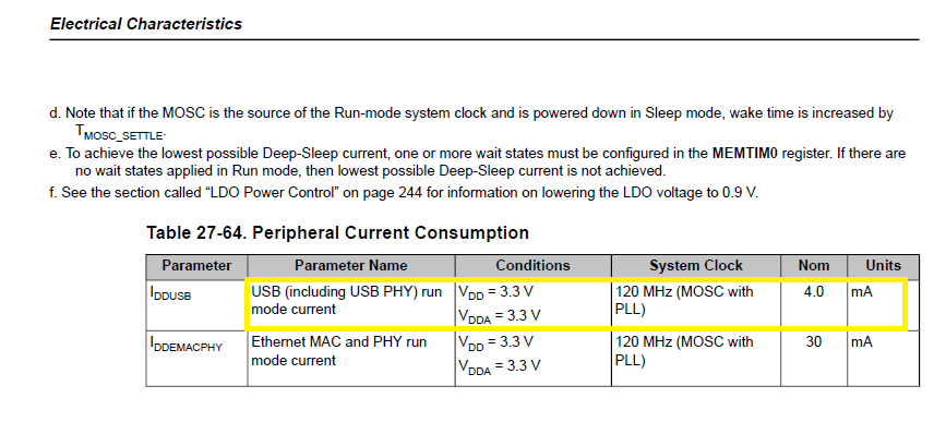
Is the MCU internal +2v2 LDO the source for USB0 power ? is it possible choice 3.3uf being excessive should PWM0 produce transient upon VDDC? What are recommended VDDC cap values under typical MCU conditions PWM0 drives HV inverter? Would not that have been determined based on laboratory testing of VDDC with PWM0 actually driving a HV inverter? Such is questionable datasheet disclosure MIA or are we expecting far to much today? 

  • Hello BP101,

    BP101 said:
    Is the MCU internal +2v2 LDO the source for USB0 power ?

    I don't have enough depth about internal hardware to comment on that, sorry.

    BP101 said:
    Would not that have been determined based on laboratory testing of VDDC with PWM0 actually driving a HV inverter? Such is questionable datasheet disclosure MIA or are we expecting far to much today?

    I think you overestimate the breadth of device testing when making specifications. Especially given an application like yours was more of a periphery interest for the device given the prominence of C2000 processors handling motor drive applications leaps and bounds better than our own.

    We have never made such tests. You are certainly expecting far too much on that front today.

    BP101 said:
     is it possible choice 3.3uf being excessive should PWM0 produce transient upon VDDC? What are recommended VDDC cap values under typical MCU conditions PWM0 drives HV inverter?

    That's something you need to determine on your system, it could be possible but how are we to be able to comment on the level of transient and what affect the 3.3uF cap would have? This is a system specific concern that you need to evaluate further. Especially so if you believe the issue is from VDDC noise.

    If there is noise on VDDC then the result isn't exactly surprising to me. After all, it is generally expected that reasonably clean voltages are supplied to the device. After all if it had no issue with noise and transients on the voltage times then why even bother with filter caps?

    Unfortunately, there is far too little data here to offer more pointed feedback, but if you can track the voltage swings caused by the transient then maybe we can offer further comments.

  • Hi Ralph,

    Where does USB0 peripheral get it's internal power rail from does not seem an overly complicated question. If TI does not know this question who does and why is it not being properly illustrated in datasheet?

    How would anyone earth trouble shoot this issue without having prior knowledge of USB0 power rail via MCU pins? Seems a bit of a cop out on TI headquarters part to not provide detailed power rail illustration for peripherals even to support personnel.

    FYI:
    Stellaris MCU predates Piccolo controller designs via TI acquired Luminary Micro's motor RDK using the LM3S8971 with Ethernet GUI control. The EK-TM4C1294XL MCU placed on warping 4 layer PCB is not best practice. So TI forum is baffled when anyone has issues with 2 layer PCB as highly capacitive X11/BPXn headers jumper wires are removed from the equation of custom PCB designs using low warpage 2 layer FR4 substrates.
  • BP101 said:
    Yet quickly disconnects endpoint either way split potentials from linear supply bucks/+3v3 LDO to MCU and PWM inverter.

    Say  What?      

    Crack staff  (never moi) asks:     (and yes - we are 'in the shop' - working away today - 'SAT.')

    • did the proofreader,  'Call in Sick?'
    • or is he/she 'blind?'
    • or speaks/reads/composes English - as 'Third or Fourth' (add on) language?

    Having past worked at a similar 'semi-giant' - I can  (completely)  second/confirm - vendor Ralph's comments!  

    Your  apparent 'belief'  - that 'EACH/EVERY' of your  'Highly Specific'  Application Demands - has been:

    • superbly  &  exactingly anticipated
    • then exhaustively tested  (w/in the vendor's laboratories)  - at/around  your  (totally UNIQUE)  Performance,  Peripheral Mix,  Power levels 
    • and (almost) matching 'your' (again) - unique board layout - component selection - software

    may prove (somewhat) of  a  'REACH'  ...  is that not so?

  • If the PWM module of MCU was not intended for HV use the datasheet had better make that very clear! Split isolated DC supplies power all kinds of embedded MCU sub systems. The TM4C peripherals should not behave differently from subsystems powered via greater potentials than MCU supply potentials being bucked down 5v to 3v3 via LDO. The MCU is not properly shielded in this case from other TI chips in the very same circuit injecting large amounts of holes into the un shielded MCU pin path.

    The EKXL launch pad seems to cover up silicon anomaly (VDDC bus) masking pin impedance to large ground plane under MCU peripheral pins connected to copper trace paths. Perhaps a multi layer substrate providing shield for potentials greater than 48v might behoove vendors silicon poor behavior?

    The norm more frequently noticed TI trying to get away with whatever it can for as long as it can, dancing around bad silicon or falsifying datasheet facts that don't hold up under testing. Easily avoidable when proper laboratory testing is done prior to mass production runs that currently expect customers to design around poorly shielded MCU peripheral pin paths is simply gambling they would.
  • Ralph Jacobi said:
    if you can track the voltage swings caused by the transient then maybe we can offer further comments.

    You have missed the point powering MCU DC rail via clean linear supply having split potentials causes immediate USB0 disconnect when PWM0 goes active. When powering both MCU and PWM sub subsystems from one DC potential up to 80vdc, there is no issue with GPTM timers or USB0. Negated to add into the post CCP edge counts similarly go bonkers too.

  • Hello BP101,

    The MCU can be used in HV applications, but it is also expected that HV systems are properly designed to not subject the MCU to excesisve transients, over voltage, over current, and other out of spec incursions. With no context of what these transients are, how am I to have any confidence that the MCU isn't be subjected to stress outside of the datasheet specs?

    By the way our LaunchPad was never designed to be used with 48V motors. Not that it can't be used with them, but the design did not consider such applications. The LaunchPad is designed for quick evaluation of all available peripherals, and the primary focuses are of USB, CAN, and Ethernet, with other focuses being UART, I2C, SPI, etc. - in general though, the differentiated peripherals which make TM4C unique to other MCU offerings by TI and at times other vendors are the focus on the LaunchPad. As such, the voltages the LaunchPad was designed for is 3-5V. Any voltages beyond that need to be addressed just like a PCB design, with proper handling to not fry the MCU with excessive voltages/currents.

    As for your last claim... intentionally falsifying a datasheet would be a notable legal offence. I don't see how you can even think ANY semiconductor company would do such a thing.

    Additionally, if this problem was a silicon issue as you claim, I imagine the amount of related problems would exceed just the single case of your system. But as always, if you can prove it out on TI hardware in a manner which we can recreate to analyze the situation, then we can assess further. It's not that the device doesn't have a notable list of items within the errata sheet... even recently, Charles uncovered another errata item which will be released formally thanks to an E2E user providing enough detail that he could analyze it and determine the device did not match DS specifications.

    I'd appreciate it if you refrain from such unfair claims when we have already spent untold hours across multiple years trying to assist you with your application.
  • Ralph Jacobi said:
    By the way our LaunchPad was never designed to be used with 48V motors

    O contraire that would be a false assumption on your part and no where documented such claim you make. Fact is we have launch pad working 165V 3 phase inverter, USB0 was not so quick disconnecting as after all the X11 jumper wires were removed. Proof enough the multilayer PCB covers up several MCU issues TI is seemingly not even aware of.

    Ralph Jacobi said:
    I'd appreciate it if you refrain from such unfair claims

    The claim was mainly in disgust for several other TI datasheets claims/specifications so far from the actual working silicon its not funny. Spending hundreds of wasted hours trying to justify printed sheet specifications that can't be answered by TI forums is no fun. Sorry if you thought it directly aimed this forum.

    Ralph Jacobi said:
    intentionally falsifying a datasheet would be a notable legal offence

    Good example is the TM4C1294 analog comparator electrical specification, VOS tested only @VREF=100mv threshold. No other REAL world threshold voltages are shown, in my opinion evades the fact the comparator threshold VREF is far to sensitive and requires VREF be far more than set mid supply.

  • We can unplug USB0 and re-establish endpoint connection after PWM0 is running and it may stay connected for a while then randomly or immediately disconnect.

    It would seem from that observation USB0 peripheral has DC noise specification, not listed in datasheet. Where USB0 peripheral sources DC is an important fact engineers need to know in order to make judgment for trouble shooting issue. To say no information on subject, an insane thought being TI logo is on the MCU.

    Note in this idea AINx Rs impedance reduces relative to larger value cap placed pin to ground. So 39n might set AC RMS impedance to 880 ohm, 1n cap 18k - 36k. TI Tina AC analysis confirms this finding the TM4C1294 datasheet seems to omit. Point is 39n adds serious roll off to the signal and produces longer hang time for transients to adversely inflict the MCU. So to say keep impedance low may be a double edge sword.

  • It would seem we are expecting far to much from the greatest silicon manufacture on earth to ask how USB0 gets it's juice to run. Perhaps its the ice cream man we need to ask such difficult questions and unlikely has the green popsicle of choice been given fair review in that cold ice box.
  • Buried deep in the bowls of datasheet lies clue we seek.  However adding TVS diode to VDD near USB0 side of MCU did not stop client disconnects.  Have to wonder if PCB frame ground to USB mini jack shield being separate AC bonded earth ground is causing analog interference. Letting PCB frame ground float made no difference to stop USB disconnect. Added 3v3 TVS diodes to all INA240 transient pulse spitting outputs, again made little to no difference in USB endpoint disconnects.

     But at least we know where USB0 gets juice from as the ice cream man gave us a green popsicle.


    The LDO Power Calibration registers, LDOSPCAL and LDODPCAL, provide suggested values for the LDO in the various modes. If software requests an LDO value that is too low or too high, the value is not accepted and an error is reported in the SDPMST register.

    Note: When using the USB, Ethernet, EPI, and QSSI interfaces, the LDO must be configured to 1.2 V.

  • E2E Users,

    Please be aware these forums are for technical support of Texas Instruments products, which we take very seriously at TI. This is not the place for sarcasm or otherwise offending others. This behavior will not be tolerated on these forums. Please keep the discussions confined to the technical issues at hand.

    If you have a legitimate complaint about the support you are receiving here, please submit a request to our Customer Support Center by clicking ‘Email TI’ here: http://www.ti.com/support

    Thank you,

    Jim Carrillo

    Manager, Online Support

    Texas Instruments

  • Hi Jim,

    I can't see any offence being posted in this thread other than finding a lack of competence on a particular subject. TI personnel should have access to all facts relative to a particular device and not make excuses or hide behind non disclosures. For TI personnel to say we don't have that information is complete nonsense.

    TI methods of acknowledging issues seem to differ from proven methods decades in making among several TI forums. Is it ok to say we have supported you but not actually provided much of any factual content, that seems more often the case. There was never the intent to humiliate anyone only to point out less than real world testing methods seem the norm here and attempting to raise the quality bar higher than it now stands!

    In this forum we see hundreds of threads custom PCB failures and more often they are not multilayer stacks for good reasons, cost being one high warpage another. Yet TI themselves make double sided TIDA for several Piccolo MCU but TM4C1294 is completely exempt from any like in kind TI testing, why is that?
  • Hello BP101,

    Based on the information you presented at the start of this thread, I had - which I realize now was incorrect - interpreted the question as asking about the inner workings of the device at an IC design level. I.E. not information disclosed in the datasheet because it is either information that either A) only the IC designers are deeply familiar with, or B) design data proprietary to our TI device. It was not clear at all to me that the only question at that time was 'which voltage rail that is input to the device is used for USB power'. Specifically my answer was to the comment of "Is the MCU internal +2v2 LDO the source for USB0 power ?", and by saying internal, that - to us as TI apps engineers - usually means IC design level content that goes beyond the datasheet and would require IC design expertise to assess and, if allowable, answer. That is why I stated that I myself did not know the inner works of the power path. I hope that clarifies better why I responded in the manner that I did.

    Now to resume the discussion on technical issues, you brought up tests you've tried from a power supply standpoint, have you also cross checked your design including the split supply based on the System Design Guidelines? www.ti.com/.../spma056.pdf

    Lastly, I don't understand what you mean by this: "Yet TI themselves make double sided TIDA for several Piccolo MCU but TM4C1294 is completely exempt from any like in kind TI testing, why is that?" Can you elaborate further?
  • Hi Ralph,

    Hey your ok many thanks for the efforts here this thread and past sorry for strange humor. Not much in the design guide regarding USB layout which were not long ago considered this custom PCB design. It would seem USB0 relies on both VDD and LDO in some way or another but how much each one, the harder question.

    Again 1.2v LDO pin 118 has 3.3uf + 100n near VDC pins, nearing 4uf shown in electrical specifications. Adding 3v3 TVS diode top of 100n near VDD on USB side of MCU pins did not help much, maybe a little. Adding TVS on 1.2v LDO would not clamp transient until 3.6v, futile to even try. EK-XL VDDC has 2.2uf + 100ns near VDDC pins and was less prone to GTO port disconnects. It don't take much of a power inflection to bounce USB0 end point even after the largest infliction has passed it remains volatile.

    Oddly GTO USB0 (EK-TM4C1294XL) would randomly disconnect end point, powered via onboard 3v3 LDO. The problem being reported past this forum was always present. In hind sight mostly cured adding 32uf electrolytic +3v3 LDO on launch pad. Custom PCB has +3v3 (TPS73533 3.3uf ceramic) powered by +24VS bucked to +5v (22uf ceramic) via 1.5Mhz Rohm switcher. Hard to imagine the bucks or LDO but perhaps cap related in some way.

    Objectionably there are no TIDI two layer PCB related gerber projects for TM4C1294NCPDT MCU. Does it not stand to reason MCU was never tested on 2 layer PCB? Thus the issues reported my be related to structure as no advisory in datasheet exists. Some behaviors are similar to EK-XL and some better, though USB0 is far worse.
  • Hello BP101,

    I'll be the first to admit I specialize more on software than hardware, so bare with me a bit on that part, but as I am trying to follow along it's hard for me to grasp all the test attempts you are making. It sounds like a lot of your tests are being done to the 1.2V LDO (which by the way is Pin 115, not 118) and 3.3V VDD line, right? And the attempts are for trying to reduce potential noise there?

    Have you been able to measure the voltage lines you are working on tweaking to see if any unusual behavior occurs when turning on the PWM? Being able to see some sort of transient would be helpful for us who don't have the in-depth system level knowledge of your board. I can't really comment based on my current knowledge whether the tests you have run are meaningful or not.

    Also, just as another train of thought, from a software standpoint, can you think of anything that occurs during the PWM starting up that would potentially block the core from processing USB critical events?

    Regarding multi-layer boards, I wasn't around at the inception or first runs of tests but I can't imagine they didn't check that out. In any case what I can confidently say is that 100's of customers use the device on 2 and even 4 layer boards and haven't had an issue, especially when following system design guidelines, so you should feel assured there isn't a device level issue with multi-layer PCB's.