Part Number: TM4C123GH6PM
Hello All,
Iam using a TM4C123GH6PM custom board. Iam trying to use the internal ADC in differential mode but somehow my ADC output is not coming correctly when I'am using multiple ADC pins.
I followed the ADC differential example and it works for single channel using sample sequencer 0.
However , When I use multiple pins with sample sequencer 2, The ADC FIFO result is incorrect as Iam getting signal only on
ui32ADC0Value[0]
ui32ADC0Value[1] is showing incorrect result.

Ia'm just testing with two input channels first.
Below is my code. Iam using timer to trigger the ADC with sampling rate as 256Hz
#include <stdint.h>
#include <stdbool.h>
#include <stdlib.h>
#include <string.h>
#include "inc/tm4c123gh6pm.h"
#include "inc/hw_memmap.h"
#include "inc/hw_types.h"
#include "inc/hw_gpio.h"
#include "driverlib/gpio.h"
#include "driverlib/pin_map.h"
#include "driverlib/sysctl.h"
#include "driverlib/uart.h"
#include "driverlib/interrupt.h"
#include "driverlib/timer.h"
#include "driverlib/adc.h"
#include "driverlib/debug.h"
#include "driverlib/fpu.h"
#include "utils/uartstdio.h"
uint32_t ui32ADC0Value[4];
uint32_t outputsamples1;
uint32_t outputsamples2;
uint32_t outputsamples3;
uint32_t outputsamples4;
void Timer0IntHandler(void)
{
TimerIntClear(TIMER0_BASE, TIMER_TIMA_TIMEOUT);
//GPIOPinWrite(GPIO_PORTB_BASE, GPIO_PIN_3, 0xFF);
ADCSequenceConfigure(ADC0_BASE, 2, ADC_TRIGGER_TIMER, 0);
//m=m+1;
}
int main(void)
{
// uint32_t ui32ADC0Value[8];
uint32_t ui32Period;
SysCtlClockSet(SYSCTL_SYSDIV_2_5 | SYSCTL_USE_PLL | SYSCTL_OSC_MAIN | SYSCTL_XTAL_16MHZ); // clock at 80 Mhz
ui32SysClkFreq = 80000000;
/*********************PIN INTILIAZATION********************************/
SysCtlPeripheralEnable(SYSCTL_PERIPH_GPIOE);
while(!(SysCtlPeripheralReady(SYSCTL_PERIPH_GPIOE)));
GPIOPinTypeADC(GPIO_PORTE_BASE,GPIO_PIN_3|GPIO_PIN_2|GPIO_PIN_1|GPIO_PIN_0);
SysCtlPeripheralEnable(SYSCTL_PERIPH_GPIOD);
while(!(SysCtlPeripheralReady(SYSCTL_PERIPH_GPIOD)));
HWREG(GPIO_PORTD_BASE+GPIO_O_LOCK) = GPIO_LOCK_KEY;
HWREG(GPIO_PORTD_BASE+GPIO_O_CR) |= GPIO_PIN_7;
GPIOPinTypeADC(GPIO_PORTD_BASE,GPIO_PIN_3|GPIO_PIN_2|GPIO_PIN_1|GPIO_PIN_0);
/*********************ADC INTILIAZATION********************************/
SysCtlPeripheralDisable(SYSCTL_PERIPH_ADC0);
SysCtlPeripheralReset(SYSCTL_PERIPH_ADC0);
SysCtlPeripheralEnable(SYSCTL_PERIPH_ADC0);
while(!(SysCtlPeripheralReady(SYSCTL_PERIPH_ADC0)));
ADCSequenceDisable(ADC0_BASE, 2);
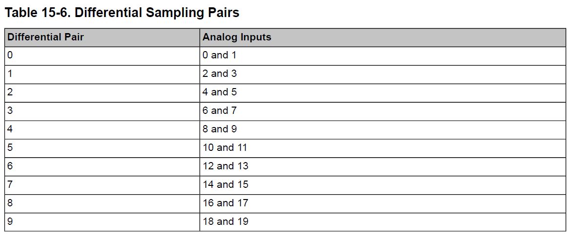
ADCSequenceStepConfigure(ADC0_BASE,2,0,ADC_CTL_D|ADC_CTL_CH0);
ADCSequenceStepConfigure(ADC0_BASE,2,1,ADC_CTL_D|ADC_CTL_CH1);
ADCSequenceStepConfigure(ADC0_BASE,2,2,ADC_CTL_D|ADC_CTL_CH2);
ADCSequenceStepConfigure(ADC0_BASE,2,3,ADC_CTL_D|ADC_CTL_CH3|ADC_CTL_IE|ADC_CTL_END);
ADCSequenceEnable(ADC0_BASE, 2);
/*********************TIMER0 INTILIAZATION********************************/
SysCtlPeripheralEnable(SYSCTL_PERIPH_TIMER0);
TimerConfigure(TIMER0_BASE, TIMER_CFG_PERIODIC);
ui32Period = 80000000/256;
TimerLoadSet(TIMER0_BASE, TIMER_A, ui32Period-1);
TimerControlTrigger(TIMER0_BASE, TIMER_A, true);
IntEnable(INT_TIMER0A);
TimerIntEnable(TIMER0_BASE, TIMER_TIMA_TIMEOUT);
TimerEnable(TIMER0_BASE, TIMER_A);
IntMasterEnable();
while(1)
{
ADCIntClear(ADC0_BASE, 2);
while(!ADCIntStatus(ADC0_BASE, 2, false))
{
}
ADCSequenceDataGet(ADC0_BASE, 2, ui32ADC0Value);
outputsamples1 = ui32ADC0Value[0];
outputsamples2 = ui32ADC0Value[1];
outputsamples3 = ui32ADC0Value[2];
outputsamples4 = ui32ADC0Value[3];
}
}
Kindly suggest a solution.