Part Number: EK-TM4C1294XL
Other Parts Discussed in Thread: INA240, TM4C1294KCPDT, LM94022
Some things become clear CH16 on two different external analog input uses have voltage coming out PK0 pin 18 when ADC0 SS1 or SS2 is being active with PWM0. We avoided using CH0 for errata #13 PE3 (AIN0) pin 12, but have issues with PK0 measuring analog sensor voltages correctly even when pulled down via 10k or less. There is no other configuration of PK0 other than it being an analog input. Oddly when ADC SS1 or SS2 are idle, PK0 is slowly cycling up and down between 602mv and 0.5mV. I think something wrong PK0 even when it is being pulled down via 10K or 3K9 it remains cycling.
On EK-TM4C1294XL re-checking AINx configuration for INA240 current monitor software formulas is impossible with voltage coming out PK0 even when being pulled down it effects the analog measurement.
On custom PCB TM4C1294KCPDT GPIO PK0 (AIN16) ADC1 inputs data from LM94022 temp sensor, goes nuts without 3k9 pull down any PWM0 activity. Yet ADC1 AIN9 GPIO PK1 PE4 2nd LM94022 quiet as a church mouse with PWM0 activity. Also had to make hardware averaging 32x in order to get any kind of stable reading from PK0 even with 3k9 pull down. Also PK4/5 are being used for PWM0, PK0 is right next to PE4 and is not noise related. PK6/7 are being used for M0Faults inputs. Sure seems like a GPIOPinConfigure() ADCSSEMUX set channel code assignment, ADC1 CH16 has some kind of decode overlap with another ADCSSMUX assignments of ADC0 CH1.
Can not find any configuration overlap GPIO PK0 for it to output voltage both MCU's PK0 AIN16. Seemingly a good clue the analog MUX versus PWM0 digital MUX has some kind of internal overlap near PK0.
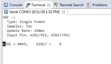
Please check a launch pad PK0 configured ANI16 of ADC0 SS1 or SS2 has any output voltage being produced or what may cause that to occur?