Part Number: EK-TM4C1294XL
Other Parts Discussed in Thread: INA240
How is it possible for C+ language to read reserved register bits 31:16 into a int32_t variable array yet only the lower bits 11:0 are marked as R0 in REG17,18,19,20? Why would Tivaware attempt to read reserved register bits in FIFO registers? Better yet is the Thumb instruction set somehow not allowing register reads in reserved space? If so how might uint32_t variable transfer effect the complied application attempting to crash in on the upper 31:16 bits of REG17,18,19,20 when they were not invited to the party? Is the FIFO read a 1:1 triggered level event into any C+ array variable cell, it would seem not always the case in any sequencers above 0.
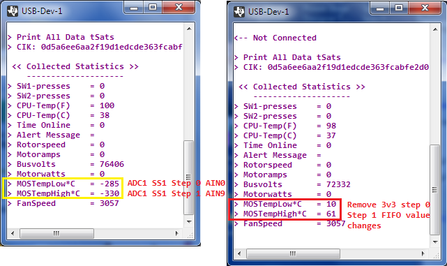
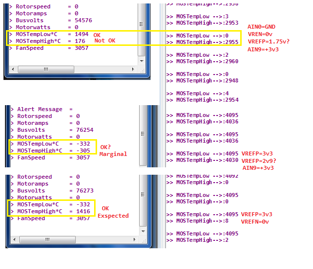
HWREG 32 macro reads into these registers via proper uint16_t variable array are not returning FIFO step 0 results data from all sequencer 1 or 2 configured steps. Typically only step 1 or 2 when being read into an uint16_t array is not the intended data via typical interrupt handling of the FIFO. It would seem the ability to properly read any single step of a circular FIFO as datasheet marginalizes has left out many details of when exactly the Head or Tail pointers change after sampling has occurred. Everyone simply assumes the tail pointer is returned to step zero upon END IE of the last step sampled. Yet the datasheet leaves all such required details to making suppositions, most of which are incorrect or not producing consistent results in all sequencers. Tivaware crude ADCSequenceDataGet() attempts to push the envelope for producing useless function calls. Please write the FIFO read data function for proper business use that it may pass any single step variable to retrieve any single data step in the sequencer into an C+ uint_16 array without retuning all FIFO steps data. If it can not do that simple step on all sequencers there is an issue with the M4 ADC that the M3 did not have.
Tivaware example projects using while(1) wait loop interrupt handling is not a safe nor practical way to handle NVIC interrupts to retrieve FIFO data in any robust application. Please use proper NVIC handling of interrupts in future example software typical of the method used in business applications of any MCU. No body is going to use while(1) loops in an large application waiting for an interrupt to occur from a triggered ADC sampling, from GPTM, PWM0, PWM1, GPIO or any other trigger source possible. That alone makes the while(1) loop more of a lower programming form thus wasting valuable CPU time and teaching bad programming methods! Again while(1) loops is not a good way for TI engineers to confirm there are not underlying issues with the ADC modules. Perhaps TI is aware odd behavior exists M4 ADC sequencers and are attempting to change the narrative of typical and proper ADC peripheral use attempting to cover them up via ADCSequnceDataGet()?
The ADC trigger is supposed to activate sampling conversion which it does for sequencer 0 steps in orderly manner but seems to often skip step 0 or 1 in SS1 or SS2 (ADC0/1), not sure about SS3. Tivaware omitting any ability to retrieve a specific sequencer step seems a bit deceptive. Underlying behavior also exists in ADC0 sequencers, ADC1 controls 19:16 channels causing issues between ADC0 & ADC1 sharing control seemingly being missed in Tivaware control over analog MUX in not 1 but 2 ADC modules. It would seem much needed information was omitted relative to how ADC0 and ADC1 can retrieve specific FIFO data of any channel as the M3 could easily accomplish via a single ADC. There are problems in the ADC modules configuration not being disclosed in the errata document.