This thread has been locked.

If you have a related question, please click the "Ask a related question" button in the top right corner. The newly created question will be automatically linked to this question.

EK-TM4C1294XL: Digital COMP data pathway

Guru 56238 points

Part Number: EK-TM4C1294XL

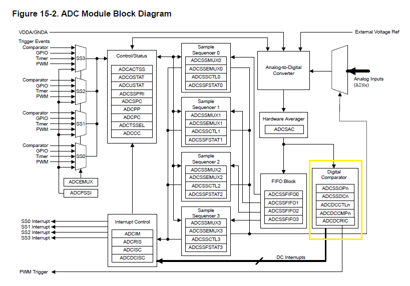
It would seem the 8 digital comparators in each ADC module must be assigned to a sequencer order to align the step to ANIx conversion input source data, contrary of Fig.15-2 and datasheet text. Tivaware version 2.1.0.12573 and 2.1.1.71 have no ability to properly configure the digital comparator with anyone of the modules 8 comparators relative to AINx analog source.

Yet when an existing FIFO steps AINx is OR'd to an relative comparator the FIFO of those steps remains in overflow. Even when ADCComparatorConfigure() and ADCRegionSet() have been configured there is no way to assign AINx conversion data to anyone of 8 digital comparators without calling ADCSequenceStepConfigure() in yet another sequencer. Without doing the latter the OR'd step with ADC_OMP_n pushes conversion data into the FIFO causing the overflow condition reported above.  

Why does digital comparators analog source require it to be OR'd to a relative AINx of existing steps matching the analog signal? Fig.15-2 indicates sequencer FIFO as being an option, not the path for digital comparators data. That makes ADCSequenceStepConfigure() an option to include digital comparators, not the explicit method to configure them to an AINx source as the only means to do so. 

ADCsequenceStepConfigure() states to logical OR one of the digital comparator selects (\b ADC_CTL_CMP0 through \b ADC_CTL_CMP7). Again that causes perpetual FIFO overflow and can't be right according to Fig.15-2 and statements in Operational modes (15.3.7.2) suggesting the AD converters data bypasses the FIFO completely. Why is ADCSequenceStepConfigure() the only way to (bind) the AD converters AINx analog signal pathway to any one of 8 digital comparators? 

15.3.7 Digital Comparator Unit:
An ADC is commonly used to sample an external signal and to monitor its value to ensure that it
remains in a given range. To automate this monitoring procedure and reduce the amount of processor
overhead that is required, each module provides eight digital comparators.

  • Hi BP101,

    I am not sure what you are doing that is causing you to get FIFO overruns. I have attached a simple project that uses two of the comparators in ADC0 on channel 0 (PE3). I never read the FIFO and it always stays empty.

    /cfs-file/__key/communityserver-discussions-components-files/908/ADC0_5F00_Comparator.zip

  • Hi Bob,

    Your configuration example miss the point being made in this thread. It should not even be necessary to configure a sequencer step as being done in the example you provided. Sequencers are intended to (bind) AINx channels to FIFOn so it should be possible to OR the digital comparator to an existing sequencer step without causing under/overflow conditions in the ANIx FIFO data. The simple fact the digital comparator is being (bind) to ANix with actual analog data being processed somehow causes ADCOSTAT/ADCUSTAT flag conditions and no FIFO data retrieved in the ADCSSFSTAT TPTR next read indicator. Asserting a check of ADCSSFSTAT TPTR is the correct way to retrieve ANIx channel data into an C+ array step.

    Again my point is we use AIN channels FIFO data in a configured sequencer but don't want to OR digital comparators to the AINx of that same sequencer or any other sequencer with a FIFO.

    According to datasheet circuit analysis Tivaware digital comparator functions (above post) like wise ADCSequenceDataGet() do NOT properly Assert or configure ADC0/1 on the silicon level. Tivaware configured sequencer FIFO's for one are running unconstrained against the steps that are being configured for specific channels, e.g more than one AINx step. The ADC digital comparators should not be forced binding association to a previously configured sequencer FIFO. Again Tivaware forces an OR'd FIFO configuration in yet another sequencer just to gain access to the digital comparator.

    The word Kludge comes to mind and so many of them have been discovered in this area of Tivaware sequencer configurations that have multiple sequencer steps with bindings to multiple AINx. Past reported digital comparator issue this forum, seemingly Amit did not understand the severity of the issue. We merely configured another sequencer with the AINx channel OR'd to the digital comparator. 

    Having double configurations for analog signals that also require digital comparators for the same ANIx channels causes Rs impedance issues. The digital comparators do not use the same TRIGGER as do the ANix channel signals. That being another point a 1 second trigger source intervals somehow align with ADCSSFSTAT TPTR/HPTR being constrained via interrupt handlers POP of individual steps into Array levels. Faster sequencer trigger intervals (PWM0/GPTM) cause random TPTR/HPTR rolling past any Asserts querying the index so the ANix channel data is being missed in the interrupt handler. Stellaris M3 team reprogrammed a single sequencer step for sampling multiple AINx analog data on the fly, seemingly to overcome issue of Rs impedance changing from having pre-configured sequencer steps to preform the same AINx samplings.  

    The FIFOn ADCSSFSTATn HPTR/TPTR are not being constrained by the sequencer step configurations and randomly roll like a roulette wheel. Your other posted example of ADCSequencerDatatGet() configured for multiple AINx analog signals is not reading the correct AINx channel and instead returns the same VREFP-VREFN data for all AINx channels with or without an analog signal.  

  • Hi Bob,

    This HWREG below makes more relative since to Fig. 15-2 FIFO being separate from digital comparators. There appears to be no overlap AINx analog channels from binding digital comparators. However it past required use of another sequencer as the ADCSSOPn traffic COP of AD converter directing data into FIFO or digital comparator but not to both in a single sequencer step via ADCSequenceStepConfigure().

    The operation below binds COMP0/1 of SS1 on the digital side of the converter versus the analog side of past SS2 configured steps. Hard to know if ADCSequenceStepConfigure() was binding the digital comparators to existing sequencer steps in SS1 by OR of ADC_CTL_CMP0 to AINx in a single configuration step. The ADCU/OSTAT in the interrupt handler was flagging a perpetual condition when AINx was OR'd to ADC_CTL_CMP0/1 in steps 0/1 of SS1. Apparently it is not straight forward when we want to branch the same sample two directions on the digital side of the converter via ADCSequneceStepConfigure().

    The original alternative was to configuring second sequencer SS2 with the same OR to same AINx, that false triggered PWM0 during POR via 1 second TriggerProcessor intervals.  Ideally the goal is to Bind (OR) the digital comparators (0/1) to the first configured sequencer (SS1) step 0/1 data paths on the digital side of the converter. It would seem that No trigger is required for a digital comparator in a Binding to a sequencer. 

    ADC Sample Sequence n Operation (ADCSSOPn) ADC0 base: 0x4003.8000 ADC1 base: 0x4003.9000 Offset 0x070 Type RW, reset 0x0000.0000

    Register 33: ADC Sample Sequence 1 Operation (ADCSSOP1), offset 0x070 Register 34: ADC Sample Sequence 2 Operation (ADCSSOP2), offset 0x090

    This register determines whether the sample from the given conversion on Sample Sequence n is saved in the Sample Sequence n FIFO or sent to the digital comparator unit. The ADCSSOP1 register controls Sample Sequencer 1 and the ADCSSOP2 register controls Sample Sequencer 2.

    /* Bind ADC1 SS1 step 0/1 operation respectively
      * to digital comparators 0/1 via REG33 */
     HWREG(ADC1_BASE + ADC_O_SSOP1) |= ADC_SSOP1_S0DCOP;
     HWREG(ADC1_BASE + ADC_O_SSOP1) |= ADC_SSOP1_S1DCOP;
    HWREG(ADC1_BASE + ADC_O_SSDC1) |= ADC_SSDC1_S0DCSEL_M & 0x0;//SS1 AIN0,
    HWREG(ADC1_BASE + ADC_O_SSDC1) |= ADC_SSDC1_S1DCSEL_M & 0x10;//SS1 AIN17


  • That is correct. Each conversion can be directed to a comparator or to the FIFO for that sequence. To load the FIFO and get the digital conversion, you must have the ADC convert the voltage twice, although it can be done in a single sequence. The code below uses sequence 1 to convert channel 0 three times. The first two results go to different comparator and the third result goes to the FIFO. Note that this was done all using TivaWare calls.

    void init_ADC()
    {
        GPIOPinTypeADC(GPIO_PORTE_BASE, GPIO_PIN_2);
        SysCtlDelay(80u);
    
        // Use ADC0 sequence 1 to sample channel 0 three times for each timer period
        ADCClockConfigSet(ADC0_BASE, ADC_CLOCK_SRC_PIOSC | ADC_CLOCK_RATE_FULL, 1);
    
        SysCtlDelay(10); // Time for the clock configuration to set
    
        IntDisable(INT_ADC0SS0);
        ADCIntDisable(ADC0_BASE, 1u);
        ADCSequenceDisable(ADC0_BASE,1u);
        // With sequence disabled, it is now safe to load the new configuration parameters
    
        ADCSequenceConfigure(ADC0_BASE, SEQ1, ADC_TRIGGER_TIMER, 0u);
        ADCSequenceStepConfigure(ADC0_BASE,SEQ1, 0u, ADC_CTL_CH0 | ADC_CTL_CMP0 );
        ADCSequenceStepConfigure(ADC0_BASE,SEQ1, 1u, ADC_CTL_CH0 | ADC_CTL_CMP1 );
        ADCSequenceStepConfigure(ADC0_BASE,SEQ1, 2u, ADC_CTL_CH0 | ADC_CTL_END );
    
        ADCComparatorConfigure(ADC0_BASE, 0, ADC_COMP_INT_HIGH_HALWAYS);
        ADCComparatorConfigure(ADC0_BASE, 1, ADC_COMP_INT_LOW_HALWAYS);
        ADCComparatorRegionSet(ADC0_BASE, 0, TRIGGERLEVEL - 128,TRIGGERLEVEL);
        ADCComparatorRegionSet(ADC0_BASE, 1, TRIGGERLEVEL - 128,TRIGGERLEVEL);
        ADCComparatorReset(ADC0_BASE, 0, true, true);
        ADCComparatorReset(ADC0_BASE, 1, true, true);
        ADCComparatorIntEnable(ADC0_BASE, SEQ1);
    
    
        ADCSequenceEnable(ADC0_BASE,SEQ1); //Once configuration is set, re-enable the sequencer
        ADCIntClear(ADC0_BASE,SEQ1);
        ADCIntEnable(ADC0_BASE, SEQ1);
        IntEnable(INT_ADC0SS1);
    
    }
    

  • Hi Bob,

    I added some info above post that may clear up why a second analog sample should not be required. If the data is already on the digital converters output bus branching into the digital converter comparator and FIFO as shown Fig15.2. We should be able to bind a second SSOP2 to the first configured sequencer on the digital side.

    The problem is ADCSequenceStepConfigure() assigns the same ADCSSOP as the sequencer FIFOn. That method seems to cause an overlapping configuration on the analog side of the AD converter versus OR-ing on the digital side only.

  • Below Fig. 15-5 shows the digital comparator blocks are not part of the sequencer configuration. Stands to reason ADCSequenceStepConfigure() is making a good effort yet falls short in properly configuring digital comparators.

    It also is not constraining ADCSSFSTATn HPTR/TPTR to the specific steps of the sequencer in the buffered data. It would seem there is missing control configuration of the FIFO steps thus it runs wildly out of control from the application attempting to place constraints via ADCSSFSTAT TPTR during high speed FIFO data transfers. What is the point of configuring sequencer steps to specific AINx channels if the FIFO index is ignoring the steps. The ADCSSFSTAT TPTR is running through the entire FIFO index no matter if the step is configured or not.

  • Hi Bob,
      
    Tivaware step configure sets the same ADCSSOP registers as HWREG directives above attempt to do. Yet OR'ing typical comparator defines in a single sequencer steps 0/1 does not seem to work as designed. HWREG Calls above seem to prove Tiva logic should be gating coincident conversion data in any step on the digital side of ADC_O_SSOP1 being OR'd. Somehow step configure bug produces a differential input via (ADC_O_SSCTL1) register of another sequencer in an opposite ADC module, to make things more confusing than ever. That really messes up the intended path of data flow during FIFO interrupt handling. 
     

  • Bob Crosby said:
    The first two results go to different comparator and the third result goes to the FIFO. Note that this was done all using TivaWare calls.

    Yet step 0 causes perpetual over/under flow in the FIFO if it is being read during interrupt handling. So Tivaware can not OR the digital comparator onto the analog FIFO in a single sequencer without overflow occurring in step 0 even after adding step 2 in your example.

    Odd fact any overflow occurs in any step used to detect digital low/high crossing of the two defined regions. Though it does not cause overflows step 0/1 (analog) with steps 2/3 made (digital) OR as you did in step 0/1. That seems an agreeable WA in this issue yet odd things still occur in other sequencers AINx channels that can not be easily explained away by Tivaware calls. 

    The FIg15-2 (yellow box) above shows digital comparators prior to FIFO's and sequencers. Position yellow box is what makes everything false narrative about requiring FIFO for adding digital comparators. Let alone it requiring a trigger source or even being configured via ADCSequenceStepConfigure().