This thread has been locked.

If you have a related question, please click the "Ask a related question" button in the top right corner. The newly created question will be automatically linked to this question.

ADC full scale trigger source PWM0/GPTM

Guru 55913 points
Part Number: TM4C1294KCPDT
Other Parts Discussed in Thread: EK-TM4C1294XL, INA240, LM94022

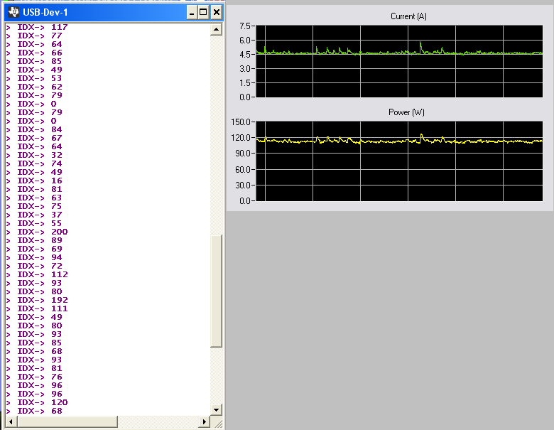
It would seem datasheet Fig.15-9 is not telling the truth when consistent periodic samples return decimal value 20-33 for analog signal of 400mV-600mV. The VREFP full scale somehow becomes 8096 and half of VREFP (1.65V) making 203uV LSB resolution (8096/1v65) in the process of what ever causes the ADC scale to change. Seemingly the PLL derived SYSCLK (120mHz) and ADC sample CLK (30mHz) are in no way synchronous with divided PWM clocking (60mHz), proved in configuration further explained.

Past experience with M3 ADC/PWM triggers reveal It should not take 48000-57600 SYSCLK ticks of GPTM one shot to trigger acquisition pulses from PWM generators 80-25us periods, yet it does! The sequencer trigger timing from PWM0 GEN0 configured (PWM_TR_CNT_LOAD) is so far from center pulse periods ADC acquisitions it's dysfunctional as a trigger source for phase current detection! That is why a GPTM one shot ADC trigger source is now required to find the PWM period centers that GEN0 trigger load being (Asynchronous), GEN0 trig load count method industry choice of engineers. 

The evidence is overwhelming settled acquisitions were being missed and scaled incorrectly at the same time even when not being missed. Still far to many 0's are AD converted in the POP data read from different configured FIFO's from PWM AD conversions of inductive current monitors. However the very limited incorrectly scaled sporadic FIFO data can build a monotonic ratio metric slope in 1/2 scale (8096/2 +1v65) via internal VREFP configured +3v3, baffling! Further evidence the PWM0 GEN0 trigger source that once worked correctly (M3) code to target center of ADC analog samples synchronous to/with PWMCLK fails in the M4 code with typical configured PLL clocks.

Some how the timing of the ADC module (120mHz) and PWM module (60mHz) divided clocks are to far apart and cause ADC trigger source timing issues, why? How can the VREFP full scale be so far from correct (8096/2 +1v65) for RAW data POP's to C+ array? Verified at times both linear and periodic analog signals are producing very low scale results data, counter to internal reference VREFP=3v3. How and why is the ADC scale being effected in most all configured sequencer steps that high speed trigger source from GPTM, PWM0 and even low speed PROCESSOR?

Obviously these 2 questions require LAB time for TI engineers as the issues encountered are repeatable EK-TM4C1294XL in ADC0, PWM0 configurations. Similar symptoms are posted several different ways before finally realizing above issues and narrowing down VREFP 3v3 full scale is (randomly) being changed during analog acquisitions, disregarding ADC internal reference configuration.

  • The VREFP scale is off by nearly 200 counts in most values above capture 0-400mV analog signal. The RAW POP was done cyclical (sequencer step 0,1,2) printing results data relative to PWM0 PWMENABLE register alignment with ADC sample triggers via GPTM4A on targets of PWM GEN0,1,2 pulse centers GPTM one shot loaded 45000-57600 SYSCLCK ticks (@8.333ns) in triggered conversions.

    Perhaps the PWM module clocking is still to far away from the ADC module clocking making it asynchronous in the process? The odd part is triggering is supposed to synchronize data but the AHB don't seem to care about inter module triggering!
  • BP101,

    Your claims against our part are quite serious. We have not had anyone make similar claims. You claim these results are reproducible on an EK-TM4C1294XL. Please provide the project that I can use to examine your claims. I strongly suspect there is an error in the configuration of your software or hardware.

  • Hi Bob,

    We have to first be aware a condition occurs as several posts have tired to convey simple tests with 102Hz GPTM cause the presumed 0-4096 full scale to divide in half. Past revision datasheet suggest 2MSPS was 6096 full scale but it seem 8096 full scale is more fitting for the values the POP is returning. That poor POP value suspected Thumb roots past extended into M3 Stellarisware but was covered up via software call shown below. It effectively creates stacked POP integer values by extending the index multiple levels deep across several array with the same name.

    Configuring SYSCLK to 60mHz to match PWM 60mHz and ADC made no difference in triggered conversions RAW POP values being anywhere close to the 200 range. Oddly clocking sequencer trigger source GPTM via PIOSC locks up MCU even with 120mHz SYSCLK. GEN0 triggered conversion is in no way synchronous to the real inductive current being produced. I will work on the EK example since now being aware of what is causing the failure in past software and M3 that TI endorsed when merging with LMI. 

    Would you agree if a trigger source can not create any monotonic trace slope it has missed acquisition settling of the periodic analog signal?   

    Setting the PWM output GPTM one shot sequencer trigger for 57K SYSCLK ticks delay gets the current slope even closer to the real thing. The problem remains low acquisition values, were past overcome by LMI software accumulating array data via insane software index POP (below). That method causes incorrect closed loop current measures and mayhem in the process but you can see how high the values get below.

     g_psPhaseCurrent = ui16PhaseRaw[g_ucCurrentIndex] = g_sMotorCurrent;

    Recall capture below  is 700mA peak LMI code TM4C in the scope widget but DMM was 1.2-1.5 Amps. POP code above adds the g_sMotorCurrent into the FIFO data, numbers are FUDGED!  


  • BP101 said:
    simple tests with 102Hz GPTM cause the presumed 0-4096 full scale to divide in half.

    There is no circuit inside of the TM4C1294 that intentionally does this. If you are only seeing this on the low end scale (200-600mV), I think a much more likely scenario is that you are capturing noise spikes. Remember that any loop antennae (which includes PCB traces and jumper wires) will collect an induced voltage in the presence of a changing magnetic field. A switching current in a wire will cause a changing magnetic field. Switching large currents such as in driving a motor is very likely to cause electrical noise on your ADC conversions. So here are some questions to help you verify if your conclusion is correct. Do you see the same scale change (2x or 4x) when converting voltages near the midpoint (1.65V)? Do you see the same variation when you are not switching currents?

    BP101 said:
    Past revision datasheet suggest 2MSPS was 6096 full scale but it seem 8096 full scale is more fitting

    Can you point me to the revision and location? Was it a past revision of the datasheet for this part?

    BP101 said:
    the values the POP is returning

    By "POP" do you mean the values read from the FIFO?

  • POP is datasheet term for circular FIFO read event by software. The 6096 was past datasheet and removed in later revision. I can make the POP's create same high values, LMI was creating fuzz line moving in Widget, smoked several disk drive motors with that approach. That is not true acquisition, it is simulated ratio metric amplifier noise full of errors, similar to multiplying PWM duty cycle into array data of smaller value acquisition conversions.

    Really want to achieve a correct measure of 10mV/Amp INA produces. ADC can not lock on to the acquisition peaks remain unsettled in the converters view no matter NSH value. ADC seems to sample the entire signal disregarding VREFP 3v3 full scale being a factor.

    Adding 480 into the POP's RMS filter we get a simulated linear slope up to 4.6-4.8 amps and very little below that during deceleration maybe 100mA. For the little motor 200-400mA had to add decimal 25 as a base line. That need to add digital slope adding specific decimal values to counter acquisition failure is the biggest clue of all. So adding decimal 25 as base for 4.6 amp below would be move like 1.2 amp in the scope widget so had to add 480 to get it up where the DMM shows it should be.

    Ideally we want to track the current rise/fall on the back edge of the analog signal but ADC appears to sample the entire slope down to VREFN as seen in the widget traces.  Shouldn't we expect to acquisition much higher values in the RAW FIFO data? It's not being drained in IDX capture below unless over/under flow might occur, debug print watch reports that.

    g_sMotorCurrent = ui16PhaseRaw[g_ucCurrentIndex];

  • Bob Crosby said:
    Switching large currents such as in driving a motor is very likely to cause electrical noise on your ADC conversions

    Perhaps you didn't read the INA240 has PWM transient rejection and removes larger shunt noise, besides the external filter/s even more before the AINx input ever gets a taste. Notice these are very small currents, disk drive motor 600mA startup peak. 

  • Hi Bob,

    Backing up to the EKXL/EVM again indicates HWREG POP's even by Tivaware from ADC0/1 SS1/SS2 were often noise related (no motor). The top capture results are not of the actual channel conversions as shown below. Further by not draining FIFO2 during interrupt after 1 of any 3 POP's might occur relative to PWM REG 3 PWMENABLE bits being synchronous to GPTM triggered sample data on those channels. ADC0 SS1 AIN1,2,5 having 10K pull downs to ground, POP data does not exactly match the input analog signal. Secondly LM94022 sensors require integers to produce negative signs when temp drops below zero degrees, ADCSequenceDataGet() is not even compatible with (int32_t) or (int16_t) variable therby forcing direct HWREG POP debug via TPTR as datasheet recommends does not seem consistent under all conditions. These POP problems seem C+ language related Thumb instructions to properly read the FIFO data at high speed and or unknown internal timing on AHB when trigger souring between peripherals occurs at high bus speeds. 

    The second capture below shows a potential to double VREFP 4096 full scale 8196 simply via POP of FIFO into array cell that does not align with ADCSSFSTAT TPTR of the configured step. This proves it is possible hardware can return incorrect results data that have little reference to the actual analog channel samples presumed to be occurring. Again Tivaware HWREG also used in ADCSequenceDataGet are both having same POP issues more often when the END IE period is high speed triggered via PWM0 or GPTM. However the second capture below occurs in 1 second interval TriggerProcessor but the POP array cell alignment ADC1 FFIO1 POP to array cell was purposefully set 1 above step 1, more often produced (-1) display and every so often 8193 RAW FIFO data would display (red box) for a few cycles with +3v3 input to AINx.   

    EKXL/EVM:

  • Some of the rouge POP values sequencer step 0 were due to recently switching AIN17 (PK1) to AIN5 (PD6) on EKEVM using (X11-pin 44) for testing. Also AIN5 was being configured prior to USB0 control (GPIO_PD6_USB0EPEN) digital control of U4 OGT power mode. Perhaps PD6 should not have been available on the X11 header since if AIN5 if assigned to sequencer step can some how back wash analog MUX internally sample the digital USB0EPEN signal.

    Thus removed AIN5 configuration which should never be available for use X11 pin 44. Heat of discovery forgotten PD6 was USB0EPEN yet not on our custom PCB USB0EPEN uses PA6 and PD6 configures AIN5. This PD6 unnecessarily complicated matters when back tracking failure of custom PCB using modifying earlier EVM configurations.

    The POP values of EVM sequencer step 0 AIN17 (PK1) remain high (300s) 10K pull down BP2-X6-12 even after removing AIN5 PD6 from step 0 configuration. Seemingly even PK1 is crossed with some other pin MUX configuration but is not to be found on either custom PCB or EVM!

  • The other part ADCSequencerDataGet() is not properly checking REG 7 ADCUSTAT, REG5 ADCOSTAT registers for conditions that sequencer FIFO data is/is not valid. Writes of the ADCUSTAT drop the data and return 0's as datasheet outlines, was reported several times. Tivaware ADCSequencerDataGet() is not properly checking the status registers during POP Read of FIFO data. Tivaware call above is not an acceptable method to return POP data to the application.

    This condition if left unchecked can manifest into strings of incorrect data POP into application even if the status is being cleared by the application after the events below have occurred. That draining the FIFO and returning may not reset the FIFO for the next write cycle interval of the ADC trigger source producing the conversion data.

    Register 7: ADC Underflow Status (ADCUSTAT), offset 0x018
    This register indicates underflow conditions in the sample sequencer FIFOs. The corresponding underflow condition is cleared by writing a 1 to the relevant bit position.

    SSn FIFO Underflow
    The valid configurations for this field are shown below. This bit is cleared by writing a 1.
    Value Description
    0 The FIFO has not underflowed.
    1 The FIFO for the Sample Sequencer has hit an underflow condition, meaning that the FIFO is empty and a read was requested. The problematic read does not move the FIFO pointers, and 0s are returned. 
     
    Register 5: ADC Overflow Status (ADCOSTAT), offset 0x010
    This register indicates overflow conditions in the sample sequencer FIFOs. Once the overflow condition has been handled by software, the condition can be cleared by writing a 1 to the corresponding bit position.

    SSn FIFO Overflow
    Value Description
    0 The FIFO has not overflowed.
    1 The FIFO for Sample Sequencer 2 has hit an overflow condition, meaning that the FIFO is full and a write was requested. When an overflow is detected, the most recent write is dropped.

  • BP101 said:
    ADCSequencerDataGet() is not properly checking REG 7 ADCUSTAT, REG5 ADCOSTAT

    It was not intended for the function ADCSequencerDataGet() to check overflow and underflow status. The functions ADCSequenceOverflow() and ADCSequenceUnderflow() are provided for that purpose.

  • Hi Bob,

    Certain FFIO conditions remain in underflow as discovered may affect TPTR flag by setting RWIC the ADCOSTAT/USTAT or simply draining the FIFO prior to clearing status after the POP events. Other cases FIFO must be drained and ADCOSTAT/USTAT set or the POP fails to copy any data into the C+ array step 0 when PWM0 GEN0 is the trigger source. Clearing the ADCOSTAT/USTAT was part of why ratio metric current slope was impossible to achieve being the TPTR froze up on SS1 or SS2 even when GPTM the trigger source. Guessing that caused perpetual underflows not being reported in the ADCUSTAT flag event even when ADCSequenceDataGet() was being called. It remains unclear why only SS1 and SS2 in ADC0/1 have TPTR issue when  SS0/SS3 do not when TPTR  USTAT was being cleared each interrupt cycle. 

    Seems inconsistent behavior between sequencers where the trigger source speed somehow dictates how the USTAT is handled. Oddly overflow never seems to occur and under flow without TPTR index movement produces POP data results of 0x000. There does not seem to be any control over FIFO writes other than the trigger conversion once the sequencer is enabled. The enabled  sequencers are always sampling the analog channels, not specifically being stated in the datasheet. That seems to be where SS1, SS2 underflow is stemming from. Long as we don't clear the SS1 or SS2 USTAT/OSTAT registers during the END IE interrupt the TPTR moves the index (0x0-0x3) and real time data results occur from sequencer configured channels. Sequentially draining FIFO1/2 and or clearing ADCUSTAT/OSTAT is a typical procedure after POP of all configured sequencers steps has occurred and should not cause perpetual under flows.     

  • If sequencer FIFO is not drained after each END IE cycle the FIFO decimal value creeps upward, at least it does with EK/EVM testing with 10k pull downs on AIN1,5,17 channels. Forcing the clearing of USTAT/OSTAT (RW1C) was locking the TPTR in SS1, SS2 but not in SS0.

    Draining the FIFO without first disabling or re-enabling sequencer after, keeps the FIFO digital value from growing. That increasing FIFO value likely occurs as it free runs between Triggered events. Draining the FIFO after all POPS of source data keeps FIFO digital value equal with application expected values. That FIFO behavior is not being described in the datasheet, what occurs to CADC after sequencers are enabled open or Rs high impedance AINx. Piccolo has a feature to dump the charge between cycles, described as those who insist on cheating with Cext values. Tivaware could add a FIFO drain call to keep this charge from building between sample triggers.

    The question is where is the extra CADC charge coming from, as CH8 +3v3 via 100k is far from CH1,2,17 of EK/EVM testing. Another oddity is ADC1 ADCPP REG64 indicates 24 AIN channels being available.