This thread has been locked.

If you have a related question, please click the "Ask a related question" button in the top right corner. The newly created question will be automatically linked to this question.

TM4C123GH6PM: Sampling 2 signals from GPIO analog pin using 2 channels of ADC simultaneously

Part Number: TM4C123GH6PM


Hey!

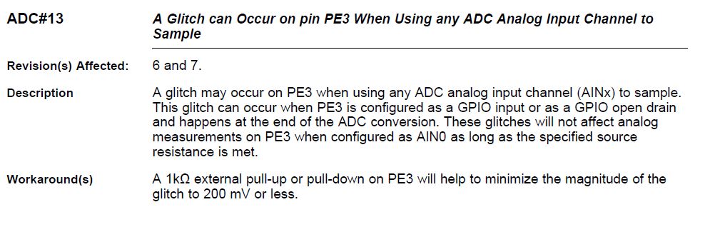
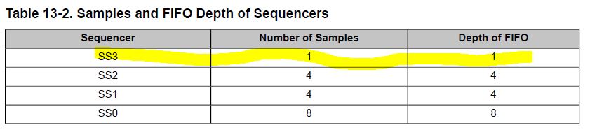
I want to input 2 different samples in 2 different analog pins (PE2 and PE3 for example) and then sample them simutaneously to print it on the UART, but I don't know how to configure the ADC. Any help? A commented code and an explanation of the functions (like - what are the sequencers, how to attach channels to the GPIO pins  and how to use ADCSequenceStepConfigure function) would be awesome! (I've tried reading some forums and the Tiva Ware Peripheral Driver's library documetation, but I could'nt achieve any of my goals. Thank you!

  • Hi,

     There is TivaWare ADC example in <TivaWare_Installation>/examples/peripherals/adc/single_ended.c . Even though this is only taking one analog input but you can extend it to taking multiple channels. I will suggest you run this example first to understand how the ADC and the TivaWare works before you extend to more than one channel. Below code is for two channels. 

        SysCtlPeripheralEnable(SYSCTL_PERIPH_ADC0);
    
    
        SysCtlPeripheralEnable(SYSCTL_PERIPH_GPIOE);
    
        GPIOPinTypeADC(GPIO_PORTE_BASE, GPIO_PIN_3 | GPIO_PIN_3);
    
        ADCSequenceConfigure(ADC0_BASE, 0, ADC_TRIGGER_PROCESSOR, 0);
    
    
        ADCSequenceStepConfigure(ADC0_BASE, 0, 0, ADC_CTL_CH0 );
        
        ADCSequenceStepConfigure(ADC0_BASE, 0, 1, ADC_CTL_CH1 | ADC_CTL_IE |
                                 ADC_CTL_END);
    
        ADCSequenceEnable(ADC0_BASE, 0);
        
        ADCIntClear(ADC0_BASE, 0);

  • Hello,

    I am also attempting to sample 2 analog signals from GPIO pins. I have applied the changes that you suggested to the TivaWare peripheral single ended example and it appears to be reading both channels.

    My issue is that I have noticed that one channel appears to affect the other substantially (crosstalk?). For instance, I will be reading ~1500 counts on Channel 0 and ~300 counts on Channel 1 and if Channel 0 increases to ~2500 counts (from a change in the input) Channel 1 will increase by ~100 counts without changing the input to Channel 1.

    Is this normal? Is there some configuration that I am missing?

    Thanks,

    Ken
  • Hi,

      There is a errata on pin PE3. See below description and the workaround. If possible, you can also avoid using PE3 for AIN0 sampling. For example, use the PE2 and PE1 on the launchpad to sample your two analog inputs.

  • Charles,

    I have switched to PE2 and PE1. That seems to have fixed my issue with the two channels affecting one another. They are however fluctuating by almost 100 counts despite having a very steady input (I have a simple set up with a couple of 1.5 volt batteries and a voltage divider to see how the channels are responding). Should I be expecting different results? Is it necessary to do hardware or software oversampling in order to obtain much more stable counts?

  • Hi,
    How did you construct the voltage divider? Without the voltage divider can you feed an input that is less than 3.3V do you see the fluctuation? You want to use a low-value resistor from the ADC input to the ground, ideally less than 1 kΩ. See the TM4C123 system design guideline in the ADC section. A low resistance helps charge-couple your input voltage to the internal sampling capacitor.

    www.ti.com/.../spma059.pdf

  • The voltage divider was previously constructed with 4.7kOhm resistors. I switched to 1kOhm and no difference. I also supplied 1.5 volt from battery directly to input and still see fluctuations of up to 60 counts. I incorporated .47ufarad capacitors as well but that did not seem to change the results either. Any other suggestions?
  • As a follow up, when I short the input to ground I get fluctuations of ~30 counts. If I hardware oversample 64 samples it stabilizes at around 10 counts and fluctuates by 1 or 2 counts.
  • It doesn't make sense to me. Do you have another board to try?

  • Hey,Charles

    Well, first of all, thank you, but there is a problem in my system. I want to attribute CH0 to PE1 and CH1 TO PE2. However, when I connect my signal source to PE3 it is also reading . What can I do to stop reading it? Here is my code:

    	SysCtlPeripheralEnable(SYSCTL_PERIPH_ADC0);//Enable the ADC0 module.
    	
    	SysCtlPeripheralEnable(SYSCTL_PERIPH_GPIOE);//Enable GPIOE for analog in
    	
    	GPIOPinTypeADC(GPIO_PORTE_BASE, GPIO_PIN_2| GPIO_PIN_1);
        
        ADCSequenceConfigure(ADC0_BASE, 3, ADC_TRIGGER_PROCESSOR, 0);
    
    	ADCSequenceStepConfigure(ADC0_BASE, 3, 0, ADC_CTL_CH0 | ADC_CTL_IE |
                                 ADC_CTL_END);														 									 
        ADCSequenceEnable(ADC0_BASE, 3);
    
        ADCIntClear(ADC0_BASE, 3);

  • First of all, you cannot use Sequencer 3 to sample more than one channel. That is already wrong. Sequencer 3 supports only one channel.  For two channels you can use Sequencer 0, 1 or 2. Fix this first and try again. I think you should get better result.

    Earlier I suggested you to try the TivaWare example as is. Did you have a chance to do that? Did you measure the voltage correctly?

  • Ok! I'll do it. Thank you again. I've also tried the TivaWare example.
  • Hey,Charles
    I've already tried the example and I've done this changes you suggested. Even though, the problem is the same - the channels are interfering in each other. Another thing is that I want to know how can I attribute channels to gpio pins, for example, how can I use channel 0 exclusevely for PE1 and channel 1 exclusevely for PE2?
    Thank you very much!!
  • Your code has another problem. See below mapping. If you want to use PE2 and PE1 then they are mapped to AIN1 (Channel 1) and AIN2 (Channel 2).

    AIN1 -> PE2
    AIN2 -> PE1

    You should have had your code like below assuming you have already change to either Sequencer 0, 1 or 2 everywhere else. Suppose you use Sequencer 0 then you will write.
    ADCSequenceStepConfigure(ADC0_BASE, 0, 0, ADC_CTL_CH1); // map AIN1 to step 0 of SS0
    ADCSequenceStepConfigure(ADC0_BASE, 0, 1, ADC_CTL_CH2 | ADC_CTL_IE | ADC_CTL_END); // map AIN2 to step 1 of SS0 and make this channel the last step in the sequencer and also generateinterrupt when the sequencer completes
  • Hey, Charles

    I've done a lot of modifications, but all my channels are interfering each other, even PE3 is doing it, although I'm not using it.

    Here's my code:

    void init_Adc(void)
    {
      SysCtlPeripheralEnable(SYSCTL_PERIPH_ADC0);//Enable the ADC0 module.
    	SysCtlPeripheralEnable(SYSCTL_PERIPH_GPIOE);//Enable GPIOE for analog in
    	GPIOPinTypeADC(GPIO_PORTE_BASE, GPIO_PIN_1);
    	GPIOPinTypeADC(GPIO_PORTE_BASE, GPIO_PIN_2);
    	ADCReferenceSet(ADC0_BASE, ADC_REF_INT);
    	ADCIntEnable(ADC0_BASE, 3);
    	ADCSequenceConfigure(ADC0_BASE, 0, ADC_TRIGGER_PROCESSOR, 0);
    	//ADCSequenceConfigure(ui32Base,ui32SequenceNum,ui32Trigger,ui32Priority)
    	//Parameters:
    	// ui32Base is the base address of the ADC module.
    	// ui32SequenceNum is the sample sequence number.
    	// ui32Trigger is the trigger source that initiates the sample sequence; must be one of the
    	// ADC_TRIGGER_∗ values.
    	// ui32Priority y is the relative priority of the sample sequence with respect to the other sample
    	// sequences.
    	ADCSequenceStepConfigure(ADC0_BASE, 0, 0, ADC_CTL_CH1);//map AIN1 to step 0 of SS0
    	ADCSequenceStepConfigure(ADC0_BASE, 0, 1, ADC_CTL_CH2 | ADC_CTL_IE |
                                 ADC_CTL_END);//map AIN2 to step 1 of SS0 and make this channel 
                                              //the last step in the sequencer and also generate
                                              //interrupt when the sequencer completes														 									 
        ADCSequenceEnable(ADC0_BASE, 0);
        ADCIntClear(ADC0_BASE, 0);
    }

  • First of your sequence number is still wrong. You wrote ADCIntEnable(ADC0_BASE, 3) which should have been ADCIntEnable(ADC0_BASE, 0).

    Secondly, ADCReferenceSet(ADC0_BASE, ADC_REF_INT) is not needed as TM4C123 has only internal reference.
  • Ok! I've changed everything but there's still interference between channels , for example, when I connect any signal source to either PE2 or PE1 the UART reads and print some signals too. Even when I connect those pins to ground it still shows a strange squarewave. What can I do?

    Here's my get samples code:

    while(!ADCIntStatus(ADC0_BASE, 0, false)) 
    {
    }
    ADCIntClear(ADC0_BASE, 0);
    ADCSequenceDataGet(ADC0_BASE, 0, &channel1);
    while(!ADCIntStatus(ADC0_BASE, 0, false)) 
    {
    }
    ADCIntClear(ADC0_BASE, 0);
    ADCSequenceDataGet(ADC0_BASE, 0, &channel2);
    				
    normalizedADC = ((float)channel2)/4096.0f;
    UARTprintf("%d\r", normalizedADC);
    UARTprintf("\n");

  • Hello,

    I just wanted to follow up with my previous inquiry. I tried another board and continued to get noise (every so often jumps from 0 to ~ 30 counts) when grounding the ADC channels that I am using. Note -This board was used in a previous project and I just ordered 2 new boards to see if the boards I have used thus far are damaged in some way. When hardware oversampling of 64 samples the grounded channels register ~10 counts and fluctuate by ~1 count. I am sticking with hardware sampling as I don't need to sample faster than ~7800 SPS (1 MSPS / 2 channels / 64 samples).

    I performed a "calibration" of the ADC channels (with hardware oversampling of 64 samples) that I am using by providing each channel with approximately GND, 1, 2, and 3 volt signals by way of a voltage divider. My results indicated an extremely linear relationship with a slight offset. For PD1 my fitted line was y = 1240.6x + 6.7236 (y is counts, x is volts). This corresponds to a full range of 3.2962 volts at 12 bit resolution. For PD2 y = 1240.7x + 5.473 corresponding to a full range of 3.2970 volts. So, very close to spec!

    My only concern now is the slight offset that is necessary and the need for significant oversampling which great reduces my maximum sampling rate (if I ever need to go faster).

    FYI I am using channels PD2 and PD1. They seem to have a very small amount of interference but pretty much negligible (less then 1 count when varying the alternate channel by its full range).

    Thanks,

    Ken
  • I don't see you call  ADCProcessorTrigger(ADC0_BASE, 0). How did trigger the conversion to start?

    I asked you before if you had tried the TivaWare example as is. Did you get correct conversion data if you tie the input to either 0V, 3.3V or 1.65V? What did you get? 

  • Well,  I'm using a timer to trigger it from another function. I've put a 5Hz in one channel it's mixing with some noise from another channel. Another thing is that all the analog pins are responding to signal inputs and are printing some values to the serial port.

  •  First of all, you never answered me if you have tried the TivaWare example. I repeat, did you get proper conversion value with the TivaWare example?

    Please also ignore the first two samples per below errata and follow the workaround suggestion.

  • Well, Charles, I've alread said that I tried the example and it worked fine. I'll try this modifications as well. Thank you one more time, you're helping me a lot!
  • I've tied the input to 3.3V and to 0V. It's printing this strange signal. (I'm using arduino serial plotter )

  • Can you show your complete code?
  • Yes!

    Here is it:

    #include <stdbool.h>
    #include <stdint.h>
    #include <stdio.h>
    #include "inc/hw_ints.h"
    #include "inc/hw_memmap.h"
    #include "driverlib/adc.h"
    #include "driverlib/debug.h"
    #include "driverlib/gpio.h"
    #include "driverlib/interrupt.h"
    #include "driverlib/rom.h"
    #include "driverlib/sysctl.h"
    #include "driverlib/uart.h"
    #include "driverlib/pin_map.h"
    #include "driverlib/timer.h"
    #include "utils/uartstdio.h"
    
    static volatile uint32_t g_ui32Counter = 0;//Timer counter variable
    
    void InitConsole(void) //UART Configuration
    {
    	//
        // Enable GPIO port A which is used for UART1 pins.
        // TODO: change this to whichever GPIO port you are using.
        //
        SysCtlPeripheralEnable(SYSCTL_PERIPH_GPIOA);
    
        //
        // Configure the pin muxing for UART1 functions on port A0 and A1.
        // This step is not necessary if your part does not support pin muxing.
        // TODO: change this to select the port/pin you are using.
        //
        GPIOPinConfigure(GPIO_PA0_U0RX);
        GPIOPinConfigure(GPIO_PA1_U0TX);
    
        //
        // Enable UART1 so that we can configure the clock.
        //
        SysCtlPeripheralEnable(SYSCTL_PERIPH_UART0);
    
        // Select the alternate (UART) function for these pins.
        // TODO: change this to select the port/pin you are using.
        //
        GPIOPinTypeUART(GPIO_PORTA_BASE, GPIO_PIN_0 | GPIO_PIN_1);
    
        //
        // Initialize the UART for console I/O.												 
        UARTStdioConfig(0, 115200, SysCtlClockGet()/*16000000*/);
    }
    void Timer0BIntHandler(void)
    {   
        //Function description ->Every time a interruption occurs
        //                       the interrupt flag is cleared , so that another 
        //                       counting until reach its overflow in a infinit loop.
        //                       Then the ADC conversion is triggered to start making 
        //                       samples to show on the UART.   
        // Clear the timer interrupt flag.
        //
        TimerIntClear(TIMER0_BASE, TIMER_TIMB_TIMEOUT);
    		// Trigger the ADC conversion.
        //
        //ADCProcessorTrigger(ADC0_BASE, 3);
    		ADCProcessorTrigger(ADC0_BASE, 0);	
    }
    void init_Adc(void)
    {
      SysCtlPeripheralEnable(SYSCTL_PERIPH_ADC0);//Enable the ADC0 module.
    	SysCtlPeripheralEnable(SYSCTL_PERIPH_GPIOD);//Enable GPIOE for analog in
    	GPIOPinTypeADC(GPIO_PORTD_BASE, GPIO_PIN_1);//channel 6
    	GPIOPinTypeADC(GPIO_PORTD_BASE, GPIO_PIN_2);//channel 5
    	//ADCReferenceSet(ADC0_BASE, ADC_REF_INT);
    	ADCIntEnable(ADC0_BASE, 0);
    	ADCSequenceConfigure(ADC0_BASE, 0, ADC_TRIGGER_PROCESSOR, 0);
    	//ADCSequenceConfigure(ui32Base,ui32SequenceNum,ui32Trigger,ui32Priority)
    	//Parameters:
    	// ui32Base is the base address of the ADC module.
    	// ui32SequenceNum is the sample sequence number.
    	// ui32Trigger is the trigger source that initiates the sample sequence; must be one of the
    	// ADC_TRIGGER_∗ values.
    	// ui32Priority y is the relative priority of the sample sequence with respect to the other sample
    	// sequences.
    	ADCSequenceStepConfigure(ADC0_BASE, 0, 0, ADC_CTL_CH5);//map AIN5 to step 0 of SS0
    	ADCSequenceStepConfigure(ADC0_BASE, 0, 1, ADC_CTL_CH6 | ADC_CTL_IE |
                                 ADC_CTL_END);//map AIN6 to step 1 of SS0 and make this channel 
                                              //the last step in the sequencer and also generate
                                              //interrupt when the sequencer completes														 									 
      ADCSequenceEnable(ADC0_BASE, 0);
      ADCIntClear(ADC0_BASE, 0);
    }
    
    int main(void)
    	{	
    		// This array is used for storing the data read from the ADC FIFO. It
        // must be as large as the FIFO for the sequencer in use.  This example
        // uses sequence 3 which has a FIFO depth of 1.  If another sequence
        // was used with a deeper FIFO, then the array size must be changed.
    		
        uint32_t channel1;//Channel 0 array
    		uint32_t channel2;//Channel 1 array
    		
    		//Variables-->>
    		uint32_t ui32PrevCount = 0;
    	//----------------------------------------------------------------------
       //Initial configurations -->
    		SysCtlClockSet(SYSCTL_SYSDIV_1 | SYSCTL_USE_PLL | SYSCTL_OSC_MAIN |
                       SYSCTL_XTAL_16MHZ);// Set the clocking to run directly from the external crystal/oscillator.
        ROM_SysCtlPeripheralEnable(SYSCTL_PERIPH_GPIOC);//Enable GPIOC for LEDs
    		ROM_SysCtlPeripheralEnable(SYSCTL_PERIPH_TIMER0);//Enable the Timer0
        ROM_SysCtlDelay(1);
    	//-----------------------------------------------------------
    	 //GPIO configurations	-->
    		ROM_GPIOPinTypeGPIOOutput(GPIO_PORTC_BASE, GPIO_PIN_5);//Configure PC5 as an output
        ROM_GPIOPinTypeGPIOOutput(GPIO_PORTC_BASE, GPIO_PIN_4);//Configure PC4 as an output
    	  ROM_GPIOPinTypeGPIOOutput(GPIO_PORTC_BASE, GPIO_PIN_6);//Configure PC4 as an output
    		ROM_GPIOPinTypeGPIOOutput(GPIO_PORTC_BASE, GPIO_PIN_7);//Configure PC4 as an output
    	//-----------------------------------------------------------
    	 //Timer Settings -->
    
    		InitConsole();//UART configurations
    		//5-Configuring Timers
    		// Configure Timer0B as a 16-bit periodic timer.->Counting until 65536
        //
        // Register timer0B handler in vector table
    		IntRegister(INT_TIMER0B, Timer0BIntHandler);
    		// Display the setup on the console.
        //
        TimerConfigure(TIMER0_BASE, TIMER_CFG_SPLIT_PAIR | TIMER_CFG_B_PERIODIC);
    		//
    		//! Important
    		//Set the Timer0B load value to 1ms. 
    		TimerLoadSet(TIMER0_BASE, TIMER_B, SysCtlClockGet() / 1000);	//Divide the clok by 1000 times
    		//                                                              that is : 160000 Hz;
        // Enable processor interrupts.
        //
        IntMasterEnable();
    		//
        // Configure the Timer0B interrupt for timer timeout.
        //
        TimerIntEnable(TIMER0_BASE, TIMER_TIMB_TIMEOUT);
    		 //
        // Enable the Timer0B interrupt on the processor (NVIC).
        //
        IntEnable(INT_TIMER0B);
    		//
        // Initialize the interrupt counter.
        //
        g_ui32Counter = 0;
    		//
        // Enable Timer0B.
        //
        TimerEnable(TIMER0_BASE, TIMER_B);
    	
    	//-----------------------------------------------------------
    	 //ADC settings -->
    		
    		init_Adc();
    		
    	//-----------------------------------------------------
    	 //Variables -->
    
    		
    		float normalizedADC;
    
    		while(1)
        {		//
            Wait for conversion to be completed.
            
    			  //ADC0
    				while(!ADCIntStatus(ADC0_BASE, 0, false)) // If the sample is ready let the uart show the values 
    				 {
            }
    				ADCIntClear(ADC0_BASE, 0);
            ADCSequenceDataGet(ADC0_BASE, 0, &channel1);
            while(!ADCIntStatus(ADC0_BASE, 0, false)) // If the sample is ready let the uart show the values 
    				{
            }
    				ADCIntClear(ADC0_BASE, 0);
            ADCSequenceDataGet(ADC0_BASE, 0, &channel2);
    				
    				normalizedADC = ((float)channel2)/4096.0f;
    				UARTprintf("%d\r", normalizedADC);
    				UARTprintf("\n");
            }
    }

  • You need to use SysCtlClockSet(SYSCTL_SYSDIV_2_5|SYSCTL_USE_PLL|SYSCTL_OSC_MAIN|SYSCTL_XTAL_16MHZ) to set the clock to 80MHz. The PLL VCO output is 200MHz and you need to divide by 2.5 to get to 80MHz. You are configuring the device to run at 200MHz with divide by one. 

  • Ok! But , why is it needed?
  • If you read the datasheet, the TM4C123 is only rated for max 80MHz operation. When you configure the clock to operate at 200MHz it is out of spec. Nothing is guaranteed to work.
  • Ok! I've changed and PD1 and PD2 are not interfering each other, but PE3 is, even though it's not configure. Another thing is that the strange noise that I've shown before is still there .
  • How are you using the PE3? Are you using the PE3 as AIN0 input to the ADC or you are using PE3 as a GPIO and see glitches? In my earlier reply I showed the below errata. Implement the workaround to alleviate the glitch or don't use PE3 when you are using other AINx channels. 

  • Hey, Charles!
    I started a new code from scratch and used the example to start, then I followed all the steps that you said to me and now everything is working fine. Thank you a lot, I would not be able to do it without your help.

    Regards,
    Bruno.
  • Hi Bruno,

    Would you mind sharing the code that you got working? I'm still having issues with mine and would like to compare.

    Thanks!

    Ken

  • Hey there,

    For sure! (Feel free to ask me anything ).Here it is:

    //*****************************************************************************
    // Bruno Ribeiro Chaves 
    // Brazil - Minas Gerais / Belo Horizonte
    // @brunorchaves1
    // project.c - Configuring the ADC0 and the UART to show samples
    //						 
    //*****************************************************************************
    
    #include <stdbool.h>
    #include <stdint.h>
    #include <stdio.h>
    #include "inc/hw_ints.h"
    #include "inc/hw_memmap.h"
    #include "driverlib/adc.h"
    #include "driverlib/debug.h"
    #include "driverlib/gpio.h"
    #include "driverlib/interrupt.h"
    #include "driverlib/rom.h"
    #include "driverlib/sysctl.h"
    #include "driverlib/uart.h"
    #include "driverlib/pin_map.h"
    #include "driverlib/timer.h"
    #include "utils/uartstdio.h"
    
    ///*****************************************************************************
    //
    // The error routine that is called if the driver library encounters an error.
    //
    //*****************************************************************************
    #ifdef DEBUG
    void
    __error__(char *pcFilename, uint32_t ui32Line)
    {
    }
    #endif
    
    static volatile uint32_t g_ui32Counter = 0;//Timer counter variable
    
    void InitConsole(void)
    {
    	//
        // Enable GPIO port A which is used for UART1 pins.
        // TODO: change this to whichever GPIO port you are using.
        //
        SysCtlPeripheralEnable(SYSCTL_PERIPH_GPIOA);
    
        //
        // Configure the pin muxing for UART1 functions on port A0 and A1.
        // This step is not necessary if your part does not support pin muxing.
        // TODO: change this to select the port/pin you are using.
        //
        GPIOPinConfigure(GPIO_PA0_U0RX);
        GPIOPinConfigure(GPIO_PA1_U0TX);
        // Enable UART1 so that we can configure the clock.
        //
        SysCtlPeripheralEnable(SYSCTL_PERIPH_UART0);
        // Use the internal 16MHz oscillator as the UART clock source.
        GPIOPinTypeUART(GPIO_PORTA_BASE, GPIO_PIN_0 | GPIO_PIN_1);
    
        //
        // Initialize the UART for console I/O.
        //
    		//UARTConfigSetExpClk(UART0_BASE, SysCtlClockGet(), 115200,
        //                        (UART_CONFIG_WLEN_8 | UART_CONFIG_STOP_ONE |
        //                         UART_CONFIG_PAR_NONE));
    														 
        UARTStdioConfig(0, 115200, SysCtlClockGet()/*16000000*/);
    }
    void Timer0BIntHandler(void)
    {
        //
        // Clear the timer interrupt flag.
        //
        TimerIntClear(TIMER0_BASE, TIMER_TIMB_TIMEOUT);
    
    		// Trigger the ADC conversion.
        //
        ADCProcessorTrigger(ADC0_BASE, 0);
    }
    
    int main(void)
    {	
    	
        //Initial configurations
        SysCtlClockSet(SYSCTL_SYSDIV_1 | SYSCTL_USE_PLL | SYSCTL_OSC_MAIN |
                        SYSCTL_XTAL_16MHZ);// Set the clocking to run directly from the external crystal/oscillator.
        SysCtlPeripheralEnable(SYSCTL_PERIPH_GPIOD);//Enable GPIOD for analog in
        ROM_SysCtlPeripheralEnable(SYSCTL_PERIPH_TIMER0);//Enable the Timer0
        ROM_SysCtlDelay(1);
    	
    	// Register timer0B handler in vector table
    	IntRegister(INT_TIMER0B, Timer0BIntHandler);
    	InitConsole();//UART configurations
        TimerConfigure(TIMER0_BASE, TIMER_CFG_SPLIT_PAIR | TIMER_CFG_B_PERIODIC);
    	TimerLoadSet(TIMER0_BASE, TIMER_B, SysCtlClockGet() / 1000);	
        IntMasterEnable();
        TimerIntEnable(TIMER0_BASE, TIMER_TIMB_TIMEOUT);
        IntEnable(INT_TIMER0B);
        g_ui32Counter = 0;
    
        TimerEnable(TIMER0_BASE, TIMER_B);		
    //-----------------------------------------------------------
        //GPIO configurations	-->
    
        GPIOPinTypeADC(GPIO_PORTD_BASE,GPIO_PIN_0|GPIO_PIN_1);//Configure PE2 as an analog-to-digital input
    
        SysCtlPeripheralEnable(SYSCTL_PERIPH_ADC0);//Enable the ADC0 module.
    
        ADCSequenceConfigure(ADC0_BASE, 0, ADC_TRIGGER_PROCESSOR, 0);
    	ADCSequenceStepConfigure(ADC0_BASE, 0, 0, ADC_CTL_CH6 /*| ADC_CTL_IE |
    															ADC_CTL_END*/);
        ADCSequenceStepConfigure(ADC0_BASE, 0, 1, ADC_CTL_CH7 | ADC_CTL_IE |
    															ADC_CTL_END);
    
        ADCSequenceEnable(ADC0_BASE, 0);
    
        ADCIntClear(ADC0_BASE, 0);
    //-----------------------------------------------------
    //Variables -->
    
        uint32_t channels[8];//ADC array --> same size as FIFO depth 
        uint32_t ui32PrevCount = 0;//Timer
    		uint32_t PD0;
       	uint32_t PD1;
      
        while(1)
        {	
    	while(!ADCIntStatus(ADC0_BASE, 0, false)) {}// If the sample is ready let the uart show the values 	
    	while(!ADCIntStatus(ADC0_BASE, 0, false)) {}// If the sample is ready let the uart show the values 	
            ADCIntClear(ADC0_BASE, 0);
            ADCSequenceDataGet(ADC0_BASE, 0, channels);
            PD0=channels[1];
            PD1=channels[0];
            
        
            UARTprintf("%4d\r",PD0);
            UARTprintf("\n");
            ui32PrevCount = g_ui32Counter;//!Important
    						
        }
    }

  • Thanks so much! Unfortunately I'm not seeing any major discrepancies in terms of how you set up your ADCs.  For some reason when I scan one channel (PD_2) by itself I get the value I expect but when I scan two channels (PD_2 and PD_1) the value of PD_2 is completely different.

    I am trying to measuring the current and voltage of a brushed dc motor with these two channels so that I can estimate the power draw of the motor.

    I've attached my code in hopes that someone might be able to help.

    #include <stdint.h> //std ints (uint8_t, uint16_t, etc.)
    #include "driverlib/adc.h"
    #include "driverlib/pwm.h"
    #include "driverlib/qei.h"
    #include "driverlib/sysctl.h"
    #include "USBprint.h"

    //
    // Number of ADC samples (~Max before RAM runs out on microcontroller)
    // Need to leave some amount of RAM on board for serial print statements
    // otherwise print statements fail.
    //
    #define NUM_SAMPLES 3000

    //
    // Number of clock ticks for 20 kHz signal (clock runs at 80 MHz -> 4000 ticks)
    //
    #define PWM_PERIOD_80KHZ F_CPU / 80000 // (80 MHz / 80000 -> 1000 ticks)
    #define PWM_PERIOD_40KHZ F_CPU / 40000 // (80 MHz / 40000 -> 2000 ticks)
    #define PWM_PERIOD_20KHZ F_CPU / 20000 // (80 MHz / 20000 -> 4000 ticks)
    #define PWM_PERIOD_10KHZ F_CPU / 10000 // (80 MHz / 10000 -> 8000 ticks)
    #define PWM_PERIOD_5KHZ F_CPU / 5000 // (80 MHz / 5000 -> 16000 ticks)
    #define PWM_PERIOD_2KHZ F_CPU / 2000 // (80 MHz / 2000 -> 40000 ticks)

    //
    // Specify speed (in seconds) in which to capture each encoder velocity value
    // Timestep for encoder
    //
    // The encoder is 12 bit resolution and therefore has 4096 counts per revolution.
    // The gearbox has a reduction of ~9.96154:1 (35*37)/(13*10).
    // The motor shaft should run at ~25 Hz.
    //
    #define ENC_TIMESTEP_S 0.001

    //
    // Global variables:
    //

    //
    // Allocate space for Time (microseconds), single-ended ADC result on CH4
    // (PD_3) (12 bit ADC counts), single-ended ADC result on CH5
    // (PD_2) (12 bit ADC counts), and quadrature encoder result (ticks per
    // encoder timestep).
    //
    uint32_t ADC_Time_buffer[NUM_SAMPLES] = {0};
    uint16_t ADC_CH5_buffer[NUM_SAMPLES] = {0};
    uint16_t ADC_CH6_buffer[NUM_SAMPLES] = {0};
    uint16_t QE_buffer[NUM_SAMPLES] = {0};

    uint16_t ui16StepDelay_ms = 500;
    uint16_t ui16PWMDutyCycle_ticks = PWM_PERIOD_20KHZ/100;

    const int ledPin = BLUE_LED; //PF_2

    //*****************************************************************************
    //
    // This function sets up UART0 to be used for a console to display information
    // as the example is running.
    //
    //*****************************************************************************
    void initConsole(void)
    {
    //
    // Initialize the serial port for console I/O.
    //
    Serial.begin(115200);
    }

    //*****************************************************************************
    //
    // This function sets up LED pin to be used for displaying status information
    // to user as the example is running.
    //
    //*****************************************************************************
    void initLED(void)
    {
    //Configure LED Pin for output
    pinMode(ledPin, OUTPUT);
    }

    //*****************************************************************************
    //
    // This function sets up the ADCs to be used for capturing readings
    //
    //*****************************************************************************
    void initADC(void)
    {
    //
    // The ADC0 peripheral must be enabled for use.
    //

    //Motor Current Sensor PD_2 (AIN5)
    //Motor Voltage Sensor PD_1 (AIN6)

    SysCtlPeripheralEnable(SYSCTL_PERIPH_ADC0);

    //
    // For this example ADC0 is used with AIN0/1 on port E7/E6.
    // The actual port and pins used may be different on your part, consult
    // the data sheet for more information. GPIO port E needs to be enabled
    // so these pins can be used.
    // TODO: change this to whichever GPIO port you are using.
    //
    SysCtlPeripheralEnable(SYSCTL_PERIPH_GPIOD);

    //
    // Select the analog ADC function for these pins.
    // Consult the data sheet to see which functions are allocated per pin.
    // TODO: change this to select the port/pin you are using.
    //
    GPIOPinTypeADC(GPIO_PORTD_BASE, GPIO_PIN_2 | GPIO_PIN_1);
    //GPIOPinTypeADC(GPIO_PORTD_BASE, GPIO_PIN_2);

    //
    // ADC needs to be disabled before configured
    //
    ADCSequenceDisable(ADC0_BASE, 2);

    //
    // Enable sample sequence 2 with a processor signal trigger. Sequence 2
    // will do up to 4 samples when the processor sends a signal to start the
    // conversion. Each ADC module has 4 programmable sequences, sequence 0
    // to sequence 3. This example is arbitrarily using sequence 2.
    //
    ADCSequenceConfigure(ADC0_BASE, 2, ADC_TRIGGER_PROCESSOR, 0);

    //
    // Set the phase delay between the trigger and the start of the sequence
    // If the trigger occurs at slightly different times on the rising edge this
    // may reduce noise in the ADC signal
    //
    //ADCPhaseDelaySet(ADC0_BASE, ADC_PHASE_0);

    //
    // Configure step 0 and step 1 on sequence 2. Sample channel 0 (ADC_CTL_CH0) in
    // differential mode (ADC_CTL_D) and configure the interrupt flag
    // (ADC_CTL_IE) to be set when the sample is done. Tell the ADC logic
    // that this is the last conversion on sequence 2 (ADC_CTL_END). Sequence
    // 3 has only one programmable step. Sequence 1 and 2 have 4 steps, and
    // sequence 0 has 8 programmable steps. Since we are doing two conversions
    // using sequence 2 we will only configure step 0 and step 1. For more
    // information on the ADC sequences and steps, refer to the datasheet.
    //
    ADCSequenceStepConfigure(ADC0_BASE, 2, 0, ADC_CTL_CH5 /*| ADC_CTL_IE /*| ADC_CTL_END*/);
    ADCSequenceStepConfigure(ADC0_BASE, 2, 1, ADC_CTL_CH6 | ADC_CTL_IE | ADC_CTL_END);

    //
    // Configure the hardware oversampling factor of the ADC
    //
    //ADCHardwareOversampleConfigure(ADC0_BASE, 64);

    //
    // Since sample sequence 2 is now configured, it must be enabled.
    //
    ADCSequenceEnable(ADC0_BASE, 2);

    //
    // Clear the interrupt status flag. This is done to make sure the
    // interrupt flag is cleared before we sample.
    //
    ADCIntClear(ADC0_BASE, 2);
    }


    //*****************************************************************************
    //
    // This function sets up the PWM to be used for motor control
    //
    //*****************************************************************************
    void initPWM(void)
    {
    //
    // Setup PWM Module
    // The Tiva Launchpad has two PWM modules (0 and 1). Module 1 covers the LED pins.
    // The PWM0 peripheral must be enabled for use.
    //

    //Pulse Width Modulated Signal is driven on PB_4
    SysCtlPeripheralEnable(SYSCTL_PERIPH_PWM0);

    //
    // For this example PWM0 is used with PortB Pin 6. The actual port
    // and pins used may be different on your part, consult the data sheet for
    // more information. GPIO port B needs to be enabled so these pins can be
    // used.
    // TODO: change this to whichever GPIO port you are using.
    //
    SysCtlPeripheralEnable(SYSCTL_PERIPH_GPIOB);

    //
    // Configure the GPIO pin muxing to select PWM functions for these pins.
    // This step selects which alternate function is available for these pins.
    // This is necessary if your part supports GPIO pin function muxing.
    // Consult the data sheet to see which functions are allocated per pin.
    // TODO: change this to select the port/pin you are using.
    //
    GPIOPinConfigure(GPIO_PB4_M0PWM2);

    //
    // Configure the GPIO pad for PWM function on pins PB6 and PB7. Consult
    // the data sheet to see which functions are allocated per pin.
    // TODO: change this to select the port/pin you are using.
    //
    GPIOPinTypePWM(GPIO_PORTB_BASE, GPIO_PIN_4);

    //
    // Configure PWM options
    //
    PWMGenConfigure(PWM0_BASE, PWM_GEN_1, PWM_GEN_MODE_DOWN | PWM_GEN_MODE_NO_SYNC);

    //
    // Enable trigger for ADC
    //
    //PWMGenIntTrigEnable(PWM0_BASE, PWM_GEN_1, PWM_TR_CNT_LOAD);

    //
    // Set PWM period to 20 kHz (Max setting for motor driver)
    //
    PWMGenPeriodSet(PWM0_BASE, PWM_GEN_1, PWM_PERIOD_20KHZ);

    //
    // Set PWM duty cycle to 1%
    //
    PWMPulseWidthSet(PWM0_BASE, PWM_OUT_2, PWM_PERIOD_20KHZ/100);

    //
    // Enable the dead-band generation on the PWM0 output signal. PWM bit 0
    // (PD0), will have a duty cycle of 25% (set above) and PWM bit 1 will have
    // a duty cycle of 75%. These signals will have a 10us gap between the
    // rising and falling edges. This means that before PWM bit 1 goes high,
    // PWM bit 0 has been low for at LEAST 160 cycles (or 10us) and the same
    // before PWM bit 0 goes high. The dead-band generator lets you specify
    // the width of the "dead-band" delay, in PWM clock cycles, before the PWM
    // signal goes high and after the PWM signal falls. For this example we
    // will use 160 cycles (or 10us) on both the rising and falling edges of
    // PD0. Reference the datasheet for more information on dead-band
    // generation.
    //
    //PWMDeadBandEnable(PWM0_BASE, PWM_GEN_1, 160, 160);

    //
    // Enable the PWM generator
    //
    PWMGenEnable(PWM0_BASE, PWM_GEN_1);

    //
    // Turn on output pins
    //
    PWMOutputState(PWM0_BASE, PWM_OUT_2_BIT, true);
    }

    //*****************************************************************************
    //
    // This function sets up the QEI to be used for motor speed measurement
    //
    //*****************************************************************************
    void initQEI(void)
    {
    //
    // Setup QEI Module
    // The Tiva Launchpad has two QEI modules (0 and 1). Module 0 covers the LED pins.
    // The QEI1 peripheral must be enabled for use.
    //
    SysCtlPeripheralEnable(SYSCTL_PERIPH_QEI1);

    //
    // For this example QEI1 is used with PortC Pins 5 and 6. The actual port
    // and pins used may be different on your part, consult the data sheet for
    // more information. GPIO port C needs to be enabled so these pins can be
    // used.
    // TODO: change this to whichever GPIO port you are using.
    //
    SysCtlPeripheralEnable(SYSCTL_PERIPH_GPIOC);

    //
    // Configure the GPIO pin muxing to select PWM functions for these pins.
    // This step selects which alternate function is available for these pins.
    // This is necessary if your part supports GPIO pin function muxing.
    // Consult the data sheet to see which functions are allocated per pin.
    // TODO: change this to select the port/pin you are using.
    //
    GPIOPinConfigure(GPIO_PC5_PHA1); //GPIO_PC5_PHA1
    GPIOPinConfigure(GPIO_PC6_PHB1); //GPIO_PC6_PHB1

    //
    // Configure the GPIO pad for PWM function on pins PB6 and PB7. Consult
    // the data sheet to see which functions are allocated per pin.
    // TODO: change this to select the port/pin you are using.
    //
    GPIOPinTypeQEI(GPIO_PORTC_BASE, GPIO_PIN_5 | GPIO_PIN_6);

    //
    // nEncoderTimerPeriod: For configuring QEI (number of clock ticks over which to measure the velocity)
    //
    uint32_t nEncoderTimerPeriod_ticks = F_CPU * ENC_TIMESTEP_S; // 80000000*0.001=80000

    //
    // Configure and Enable QEI
    //
    QEIConfigure(QEI1_BASE, (QEI_CONFIG_CAPTURE_A_B | QEI_CONFIG_NO_RESET | QEI_CONFIG_QUADRATURE | QEI_CONFIG_NO_SWAP), UINT32_MAX);

    //
    //
    //
    QEIVelocityConfigure(QEI1_BASE, QEI_VELDIV_1, nEncoderTimerPeriod_ticks); // Divide by clock speed to get counts/sec

    //
    //
    //
    QEIEnable(QEI1_BASE);

    //
    //
    //
    QEIVelocityEnable(QEI1_BASE);

    }
    //*****************************************************************************
    //
    // This function blinks the LED a number of times with millisecond delay
    // between each blink.
    //
    //*****************************************************************************
    void blinkLED(uint32_t ui32Times, uint32_t ui32Milliseconds)
    {
    //
    // Blink led
    //
    digitalWrite(ledPin,LOW);
    for(int i = 0; i < ui32Times; i++) {
    digitalWrite(ledPin,HIGH);
    delay(ui32Milliseconds);
    digitalWrite(ledPin,LOW);
    delay(ui32Milliseconds);
    }
    }

    //*****************************************************************************
    //
    // This function triggers the ADC conversion and stores the ADC reading in an
    // array of unsigned integers.
    //
    //*****************************************************************************
    void readADC(uint32_t *pui32ADCValues)
    {
    //
    // Trigger the ADC conversion.
    //
    ADCProcessorTrigger(ADC0_BASE, 2);

    //
    // Wait for conversion to be completed.
    //
    while(!ADCIntStatus(ADC0_BASE, 2, false))
    {
    }

    //
    // Clear the ADC interrupt flag.
    //
    ADCIntClear(ADC0_BASE, 2);

    //
    // Read ADC value.
    //
    ADCSequenceDataGet(ADC0_BASE, 2, pui32ADCValues);
    }

    //*****************************************************************************
    //
    // This function records and stores the ADC readings in their pre-allocated
    // buffers.
    //
    //*****************************************************************************
    void recordRawReadings(bool bRunMotorStepInput)
    {
    uint32_t pui32ADCValues[4];

    //
    // Determine if motor is to be run with step input
    // Separate For loops to maximize speed/minimize computations within loop
    //
    if(bRunMotorStepInput) {
    //
    // Set pulse width duty cycle
    //
    PWMPulseWidthSet(PWM0_BASE, PWM_OUT_2, ui16PWMDutyCycle_ticks);
    delay(ui16StepDelay_ms); //Optional delay before recording values
    }

    for(int i = 0; i < NUM_SAMPLES; i++) {
    //
    // Read ADC values
    //
    readADC(pui32ADCValues);

    //
    // Store time and ADC values
    //
    ADC_Time_buffer[i] = micros();
    ADC_CH5_buffer[i] = (uint16_t)pui32ADCValues[0];
    ADC_CH6_buffer[i] = (uint16_t)pui32ADCValues[1];

    //
    //Record Quadrature Encoder values if motor is running
    //
    if(bRunMotorStepInput){QE_buffer[i] = (uint16_t)QEIVelocityGet(QEI1_BASE);}
    }

    //
    // Set pulse width duty cycle to 1%
    //
    if(bRunMotorStepInput){PWMPulseWidthSet(PWM0_BASE, PWM_OUT_2, PWM_PERIOD_20KHZ/100);}
    }

    //*****************************************************************************
    //
    // This function sends the ADC values that are stored in the buffers through
    // the serial port for additional post processing by MATLAB.
    //
    //*****************************************************************************
    void sendRawReadings(bool bIncludeQE)
    {

    if(bIncludeQE) {
    for(int i = 0; i < NUM_SAMPLES; i++) {
    //
    // Print Time (microseconds), CH5 (counts), CH6 (counts), and
    // QE (ticks per time step)
    //
    USBprintf("%.4u,%.4u,%.4u,%.4u\n\r", ADC_Time_buffer[i], ADC_CH5_buffer[i],
    ADC_CH6_buffer[i], QE_buffer[i]);

    }
    } else {
    for(int i = 0; i < NUM_SAMPLES; i++) {
    //
    // Print Time (microseconds), CH5 (counts), and CH6 (counts)
    //
    USBprintf("%.4u,%.4u,%.4u,0\n\r", ADC_Time_buffer[i], ADC_CH5_buffer[i],
    ADC_CH6_buffer[i]);
    }
    }

    delay(5);

    //
    // Print character to indicate end of data
    //
    USBprintf("E\n\r");
    }

    //*****************************************************************************
    //
    // This function sends the ADC values that are stored in the buffers through
    // the serial port for additional post processing by MATLAB.
    //
    //*****************************************************************************
    void sendRawReadingsLive(uint32_t ui32Counts)
    {
    uint32_t pui32ADCValues[2];
    uint32_t sums[3];
    uint32_t ui32StartTime = micros();

    //
    // Set pulse width duty cycle
    //
    PWMPulseWidthSet(PWM0_BASE, PWM_OUT_2, ui16PWMDutyCycle_ticks);

    sums[0]=0;
    sums[1]=0;
    sums[2]=0;
    delay(ui16StepDelay_ms);

    for(int i = 0; i < ui32Counts; i++) {
    //
    // Read ADC values
    //
    readADC(pui32ADCValues);

    sums[0] += (uint16_t)pui32ADCValues[0]; //motor current counts
    sums[1] += (uint16_t)pui32ADCValues[1]; //motor voltage counts
    sums[2] += (uint16_t)QEIVelocityGet(QEI1_BASE);

    //
    // Print Time (microseconds), CH0 (counts), CH1 (counts), and
    // QE (ticks per time step)
    //
    // Print the sums over 244 counts
    //
    if(i % 244 == 243) {
    USBprintf("%.5u,%.6u,%.6u,%.3u\n\r", micros()-ui32StartTime, sums[0],
    sums[1],sums[2]);
    sums[0]=0;
    sums[1]=0;
    sums[2]=0;
    }
    }

    //
    // Print character to indicate end of data
    //
    USBprintf("E\n\r");

    //
    // Set pulse width duty cycle to 1%
    //
    PWMPulseWidthSet(PWM0_BASE, PWM_OUT_2, PWM_PERIOD_20KHZ/100);
    }


    //*****************************************************************************
    //
    // setup() is runs once at the start of powering on the microcontroller
    //
    //*****************************************************************************
    void setup() {
    //
    // "Most of the ADC control logic runs at the ADC clock rate of 16 MHz. The
    // the internal ADC divider is configured for 16-MHz operation automatically
    // by hardware when the system XTAL is selected with the PLL."
    //
    SysCtlClockSet(SYSCTL_SYSDIV_2_5 | SYSCTL_USE_PLL | SYSCTL_OSC_MAIN |
    SYSCTL_XTAL_16MHZ);

    //
    // Initialize all necessary modules
    //
    initConsole();
    initLED();
    initADC();
    initPWM();
    initQEI();

    //
    // Indicate initialization complete
    //
    blinkLED(3,200);

    //
    // Wait for serial terminal
    //
    delay(1000);

    //
    // Display Menu
    //
    displayMenu();
    }

    //*****************************************************************************
    //
    // loop() runs continuously immediately after setup
    //
    //*****************************************************************************
    void loop() {
    //
    //Use serial event instead
    //
    }

    //*****************************************************************************
    //
    // SerialEvent occurs whenever a new data comes in the
    // hardware serial RX. This routine is run between each
    // time loop() runs, so using delay inside loop can delay
    // response. Multiple bytes of data may be available.
    //
    //*****************************************************************************
    void serialEvent()
    {
    while(Serial.available())
    {
    //Parse serial data
    switch (Serial.read())
    {
    case 77: case 109: //'m' or 'M' was pressed to view menu
    displayMenu();
    break;
    case 76: case 108: //'l' or 'L' was pressed to run motor (printout w/o buffer)
    blinkLED(3,200);
    delay(1000);
    digitalWrite(ledPin, HIGH);
    sendRawReadingsLive(Serial.parseInt());
    digitalWrite(ledPin, LOW);
    break;
    case 67: case 99: //'c' or 'C' was pressed to calibrate ADC
    blinkLED(3,200); // Indicate start of ADC calibration
    delay(1000); // Delay one second
    digitalWrite(ledPin, HIGH);
    recordRawReadings(false);
    sendRawReadings(false);
    digitalWrite(ledPin, LOW);
    break;
    case 68: case 100: //'d' or 'D' was pressed to change delay
    blinkLED(3,200); // Indicate start
    ui16StepDelay_ms = Serial.parseInt();
    break;
    case 83: case 115: //'s' or 'S' was pressed to run motor (printout w/ buffer)
    blinkLED(3,200); // Indicate start of step input
    delay(1000); // Delay one second
    digitalWrite(ledPin, HIGH);
    recordRawReadings(true);
    sendRawReadings(true);
    digitalWrite(ledPin, LOW);
    break;
    case 82: case 114: //'r' or 'R' was pressed to run motor (w/o printout)
    blinkLED(3,200); // Indicate start
    delay(1000); // Delay one second
    digitalWrite(ledPin,HIGH); // Turn on LED
    //
    // Set pulse width duty cycle to desired amount
    //
    PWMPulseWidthSet(PWM0_BASE, PWM_OUT_2, ui16PWMDutyCycle_ticks);
    //
    // Wait a desired amount (milliseconds)
    //
    delay(Serial.parseInt());
    //
    // Set pulse width duty cycle back to 1%
    //
    PWMPulseWidthSet(PWM0_BASE, PWM_OUT_2, PWM_PERIOD_20KHZ/100);
    digitalWrite(ledPin,LOW); // Turn off LED
    break;
    case 80: case 112: //'p' or 'P' was pressed to change PWM Duty Cycle
    blinkLED(3,200);
    ui16PWMDutyCycle_ticks = Serial.parseInt();
    break;
    case 81: case 113: //'q' or 'Q' was pressed to quit program
    //Clean up
    USBprintStr("Program Ended.");
    while(1){continue;}
    break;
    }
    delayMicroseconds(100); //Wait sufficient time for new serial data to become available
    }
    }

    void displayMenu(void)
    {
    //Controller Menu
    USBprintStr("Pololu Motor Calibration Menu:\n\r\n");
    USBprintStr("c - Send ADC signals\n\r");
    USBprintStr("d - Change Step Delay (ms)\n\r");
    USBprintStr("l - Run motor (non-buffered printout)\n\r");
    USBprintStr("m - Display Menu\n\r");
    USBprintStr("p - Change PWM Duty Cycle (ticks)\n\r");
    USBprintStr("s - Run motor (buffered printout)\n\r");
    USBprintStr("r - Run motor (no printout)\n\r");
    USBprintStr("q - Quit\n\r");
    }

  • Hey,

    I think you are having the same problem that I had. You gave the wrong size to pui32ADCValues[2].

    Because you're using sequencer 2 it demands an array of 4 positions "pui32ADCValues[4]", once this sequencer choose de depth to the FIFO that is also 4 in this case. Then you have to put this:

    while(!ADCIntStatus(ADC0_BASE, 2, false))

    {

    }As many as the channels you're using. So it would be like this if you are using only two channels:

    int main()
    {
      uint32_t pui32ADCValues[4];
      uint32_t PD1;
      uint32_t PD2;
    
      while(1)
      {
        while(!ADCIntStatus(ADC0_BASE, 2, false))
        {
        }
        while(!ADCIntStatus(ADC0_BASE, 2, false))
        {
        }
        ADCIntClear(ADC0_BASE, 2);
        ADCSequenceDataGet(ADC0_BASE, 2, pui32ADC0Value);
    
        PD1= pui32ADC0Value[0];
        PD2= pui32ADC0Value[1];
    }
    

    Also, your code has too many things, try to remove it for a while and fix this adc  issue first. Another thing is to look if the channels are configure correctly , once you are using PD1 and PD2 you have to use channels CH6 and CH5 respectively.

  • Thanks for your suggestion!

    Still same results though.

    Basically what I have noticed is that the one channel is still influenced by the other. Here are a few scenarios that I have worked through:

    Ch1, Ch2

    GND, GND - When both are grounded they both register around 0 counts (good)

    GND, 1.5V - When this is applied ch1 registers about 10 counts and ch2 registers about 2000 (i.e. ch1 is being pulled up by ch2)

    GND, 3V - When this is applied ch1 registers about 20 counts and ch2 registers about 4000 (i.e. ch1 is pulled up even more and seems to have a linear relationship with ch2)

    I noticed that the relationship is a lot stronger when not hardware oversampling therefore it seems like there is a settling time necessary between sampling channels. I am trying to sample extremely quickly (500 kSPS per channel). Basically when hardware sampling is enabled and large (64) it takes 64 samples of ch1 puts it in FIFO slot 1 then 64 samples of ch2 into FIFO slot 2 therefore the second 64 samples is a whole 64 microseconds later. (This is all assuming I understand this correctly). This is what makes me think that there is some sort of settling time that needs to take place. As I decrease the hardware sampling and thus decrease the time between sampling ch1 and ch2 they get worse.

    I know that on other ADC chips for input multiplexing there is time needed to switch channels, I'm wondering if that is the case for this as well?

    Also, I was looking at the ADC section of the data sheet for TM4C123GH6PM and noticed a section about the DITHER bit (pg 806). Was wondering if that needs to be set? I tried setting it but didn't seem to make a difference.

    Lastly, I wonder if a more substantial pull-up or pull-down resistor is necessary for this application? I don't know a whole lot about this stuff but just trying to make some guesses as to what I could do to fix the problem.

    Thanks again for your insight! I'm hoping someone might be able to steer me in the right direction.