This thread has been locked.

If you have a related question, please click the "Ask a related question" button in the top right corner. The newly created question will be automatically linked to this question.

TM4C1294NCPDT: ADC port LM3S9B96 to TM4C1294NCPDT issue

Part Number: TM4C1294NCPDT

Hi,

I am using the TM4C1294NCPDT with IAR.

I did port LM3S9B96 to TM4C1294NCPDT , specially about the ADC. Looks like that I did everything ok, but I have a different conversion between the microcontrollers.

The only difference that I applied was a resistor on the adc input (TM4C1294NCPDT) as the doc says http://www.ti.com/lit/an/spma049a/spma049a.pdf

 re

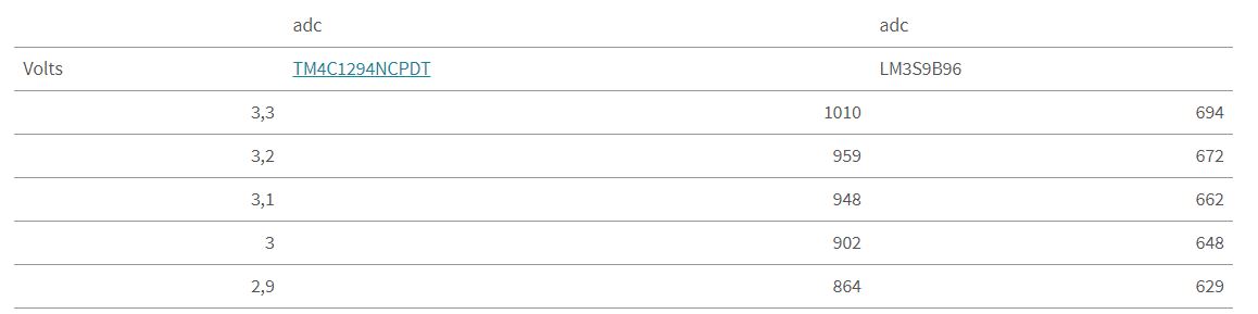
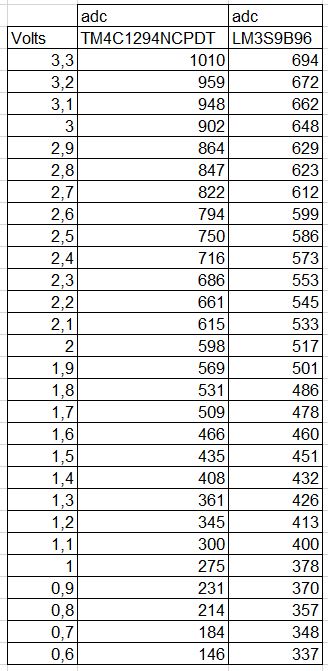
Below I put the source codes and the reads tables, by the way I know that  LM3S9B96 works in 10bits and TM4C1294NCPDT works in 12bits, so I did the conversion just dividing by 4 the TM4C1294NCPDT results.

 Please take a look, and comment will be well come.

Best Regards.

adc

adc

Volts

TM4C1294NCPDT

LM3S9B96

3,3

1010

694

3,2

959

672

3,1

948

662

3

902

648

2,9

864

629

2,8

847

623

2,7

822

612

2,6

794

599

2,5

750

586

2,4

716

573

2,3

686

553

2,2

661

545

2,1

615

533

2

598

517

1,9

569

501

1,8

531

486

1,7

509

478

1,6

466

460

1,5

435

451

1,4

408

432

1,3

361

426

1,2

345

413

1,1

300

400

1

275

378

0,9

231

370

0,8

214

357

0,7

184

348

0,6

146

337

//LM3S9B96

///----------------------------------------------------------------------------------

void main(void)

{

    SysCtlClockSet(SYSCTL_SYSDIV_4 | SYSCTL_USE_PLL | SYSCTL_OSC_MAIN |

                   SYSCTL_XTAL_8MHZ);


            SysCtlPeripheralEnable(SYSCTL_PERIPH_TIMER0);

            TimerConfigure(TIMER0_BASE, TIMER_CFG_32_BIT_PER);

            TimerLoadSet(TIMER0_BASE, TIMER_A,SysCtlClockGet()/4000);  // 250µSec

            TimerEnable(TIMER0_BASE, TIMER_A);


    SysCtlPeripheralEnable(SYSCTL_PERIPH_GPIOD);

    GPIOPinTypeADC(GPIO_PORTD_BASE, AIN9 | AIN10 |AIN11 | AIN12 |AIN1 | AIN2 | AIN3 | AIN4);


    SysCtlPeripheralEnable(SYSCTL_PERIPH_GPIOE);

    GPIOPinTypeADC(GPIO_PORTE_BASE, AIN8 | AIN7 |AIN6 | AIN5);


// Configure the ADC to

//

    SysCtlPeripheralEnable(SYSCTL_PERIPH_ADC0);

    SysCtlPeripheralEnable(SYSCTL_PERIPH_ADC1);             // ADC1

    ADCSequenceDisable(ADC1_BASE,2);

    ADCSequenceDisable(ADC0_BASE,0);

    SysCtlADCSpeedSet(SYSCTL_ADCSPEED_500KSPS);

    ADCSequenceConfigure(ADC0_BASE, 0, ADC_TRIGGER_PROCESSOR, 1); // sequencer 0 Priority 0

    ADCSequenceStepConfigure(ADC0_BASE, 0, 0,ADC_CTL_CH0);

    ADCSequenceStepConfigure(ADC0_BASE, 0, 1,ADC_CTL_CH1);

    ADCSequenceStepConfigure(ADC0_BASE, 0, 2,ADC_CTL_CH2);

    ADCSequenceStepConfigure(ADC0_BASE, 0, 3,ADC_CTL_CH3);

    ADCSequenceStepConfigure(ADC0_BASE, 0, 4,ADC_CTL_CH4);

    ADCSequenceStepConfigure(ADC0_BASE, 0, 5,ADC_CTL_CH5);

    ADCSequenceStepConfigure(ADC0_BASE, 0, 6,ADC_CTL_CH6);

    ADCSequenceStepConfigure(ADC0_BASE, 0, 7,ADC_CTL_CH7| ADC_CTL_IE | ADC_CTL_END);


//Set the second ADC

    ADCSequenceConfigure(ADC1_BASE, 2, ADC_TRIGGER_PROCESSOR, 0); // sequencer 1 Priority 1

    ADCSequenceStepConfigure(ADC1_BASE, 2, 0,ADC_CTL_CH12);

    ADCSequenceStepConfigure(ADC1_BASE, 2, 1,ADC_CTL_CH13);

    ADCSequenceStepConfigure(ADC1_BASE, 2, 2,ADC_CTL_CH14);

    ADCSequenceStepConfigure(ADC1_BASE, 2, 3,ADC_CTL_CH15 | ADC_CTL_IE | ADC_CTL_END);


    ADCSequenceEnable(ADC0_BASE, 0); // Enable sequence 0

    ADCIntEnable(ADC0_BASE, 0);  // Enable Interrupt sequence 0

    IntEnable(INT_ADC0);  //

    ADCSequenceEnable(ADC1_BASE, 2); // Enable sequence 1

    ADCIntEnable(ADC1_BASE, 2);  // Enable Interrupt sequence 1

     IntEnable(INT_ADC1SS2);


            while(1);

}          

void ADC0IntHandler(void)

{

     ADCIntClear(ADC0_BASE, 0);

            unsigned long ulData[8];    //


    // Read the data from the ADC.

    //

    ADCSequenceDataGet(ADC0_BASE, 0, ulData);

    ADCC++;

}


void ADC1IntHandler(void)

{

     ADCIntClear(ADC1_BASE, 2);

  unsigned long ulData[8];    //


    // Read the data from the ADC.

    //

    ADCSequenceDataGet(ADC1_BASE, 2,ulData);

    ADCC1++;

}


void Timer0IntHandler(void)

{

    //

    // Clear the timer interrupt.

    //

    TimerIntClear(TIMER0_BASE, TIMER_TIMA_TIMEOUT);


    ADCProcessorTrigger(ADC1_BASE, 2);

    ADCProcessorTrigger(ADC0_BASE, 0);

}


//TM4C1294NCPDT

//-------------------------------------------------------------------------------------

void main(void)

{

    g_ui32SysClock = MAP_SysCtlClockFreqSet((SYSCTL_XTAL_25MHZ |

                                             SYSCTL_OSC_MAIN | SYSCTL_USE_PLL |

                                             SYSCTL_CFG_VCO_480), 120000000);

            SysCtlPeripheralEnable(SYSCTL_PERIPH_TIMER0);

            TimerConfigure(TIMER0_BASE, TIMER_CFG_32_BIT_PER);

            TimerLoadSet(TIMER0_BASE, TIMER_A,SysCtlClockGet()/4000);  // 250µSec

            TimerEnable(TIMER0_BASE, TIMER_A);


    //

// Configure GPIO Pins PORT_B used for the Analog feedback INPUTS.

    ROM_GPIOPinTypeADC(GPIO_PORTB_BASE, AIN10 | AIN11);


// Configure GPIO Pins PORT_D used for the Analog feedback INPUTS.

    ROM_GPIOPinTypeADC(GPIO_PORTD_BASE, AIN12 | AIN7 | AIN6 | AIN5 | AIN4);


// Configure GPIO Pins PORT_E used for the Analog feedback INPUTS.

    ROM_GPIOPinTypeADC(GPIO_PORTE_BASE, AIN3 | AIN2 | AIN1 | AIN9 | AIN8); 


            ///////////////

/ Configure the ADC to

//

    SysCtlPeripheralEnable(SYSCTL_PERIPH_ADC0);

    SysCtlPeripheralEnable(SYSCTL_PERIPH_ADC1);             // ADC1

    ADCSequenceDisable(ADC1_BASE,2);

    ADCSequenceDisable(ADC0_BASE,0);

    ADCClockConfigSet(ADC0_BASE, ADC_CLOCK_SRC_PLL | ADC_CLOCK_RATE_FULL,240); //120000000/500000 = 240

    ADCClockConfigSet(ADC1_BASE, ADC_CLOCK_SRC_PLL | ADC_CLOCK_RATE_FULL,240);

    //SysCtlADCSpeedSet(SYSCTL_ADCSPEED_500KSPS);//LM3S9B96

    ADCSequenceConfigure(ADC0_BASE, 0, ADC_TRIGGER_PROCESSOR, 1); // sequencer 0 Priority 0


    ADCSequenceStepConfigure(ADC0_BASE, 0, 0,ADC_CTL_CH1);

    ADCSequenceStepConfigure(ADC0_BASE, 0, 1,ADC_CTL_CH2);

    ADCSequenceStepConfigure(ADC0_BASE, 0, 2,ADC_CTL_CH3);

    ADCSequenceStepConfigure(ADC0_BASE, 0, 3,ADC_CTL_CH4);

    ADCSequenceStepConfigure(ADC0_BASE, 0, 4,ADC_CTL_CH5);

    ADCSequenceStepConfigure(ADC0_BASE, 0, 5,ADC_CTL_CH6);

    ADCSequenceStepConfigure(ADC0_BASE, 0, 6,ADC_CTL_CH7);

    ADCSequenceStepConfigure(ADC0_BASE, 0, 7,ADC_CTL_CH8| ADC_CTL_IE | ADC_CTL_END);


//Set the second ADC

    ADCSequenceConfigure(ADC1_BASE, 2, ADC_TRIGGER_PROCESSOR, 0); // sequencer 1 Priority 1

    ADCSequenceStepConfigure(ADC1_BASE, 2, 0,ADC_CTL_CH9);

    ADCSequenceStepConfigure(ADC1_BASE, 2, 1,ADC_CTL_CH10);

    ADCSequenceStepConfigure(ADC1_BASE, 2, 2,ADC_CTL_CH11);

    ADCSequenceStepConfigure(ADC1_BASE, 2, 3,ADC_CTL_CH12 | ADC_CTL_IE | ADC_CTL_END);


    IntMasterEnable();

    ADCSequenceEnable(ADC0_BASE, 0); // Enable sequence 0

    ADCIntEnable(ADC0_BASE, 0);  // Enable Interrupt sequence 0

    //ROM_IntEnable(INT_ADC0SS0);

    IntEnable(INT_ADC0SS0);

    //IntEnable(INT_ADC0);  //

    IntMasterEnable();

    ADCSequenceEnable(ADC1_BASE, 2); // Enable sequence 1

    ADCIntEnable(ADC1_BASE, 2);  // Enable Interrupt sequence 1

    IntEnable(INT_ADC1SS2);


            while(1);

}

void ADC0IntHandler(void)

{

     ADCIntClear(ADC0_BASE, 0);

            uint32_t ulData[8];    //


    // Read the data from the ADC.

    //


    ADCSequenceDataGet(ADC0_BASE, 0, ulData);

   for(int i=8; i < 8; i++) // convert 12bits to 10bits

            ulData[i]= ulData[i]/4;


    ADCC++;

}


void ADC1IntHandler(void)

{

     ADCIntClear(ADC1_BASE, 2);

            uint32_t ulData[8];    //


    // Read the data from the ADC.

    //

    ADCSequenceDataGet(ADC1_BASE, 2,ulData);

   for(int i=8; i < 8; i++) // convert 12bits to 10bits

            ulData[i]= ulData[i]/4;


    ADCC1++;

}


void Timer0IntHandler(void)

{

    //

    // Clear the timer interrupt.

    //

    TimerIntClear(TIMER0_BASE, TIMER_TIMA_TIMEOUT);


    ADCProcessorTrigger(ADC1_BASE, 2);

    ADCProcessorTrigger(ADC0_BASE, 0);

}

///----------------------------------------------------------------------------------


  • Hi,
    I really suggest you start with the TivaWare adc and timer examples first instead of porting your LM code to TM4C129. It will be far easier for you to develop your application. I quickly glance through your code and found two issues. I didn't read your entire code though. First, please refer to the TivaWare Driver library user's guide for TimerConfigure. There is no TIMER_CFG_32_BIT_PER to be used. Perhaps this is for LM device for which I have no experience with as this is a EOL product. Second, you cannot use SysCtlClockGet() on a TM4C129 device. This is only for TM4C123 device. As I said it will be much easier if you start with the TivaWare ADC and Timer examples.

    TimerConfigure(TIMER0_BASE, TIMER_CFG_32_BIT_PER);

    TimerLoadSet(TIMER0_BASE, TIMER_A,SysCtlClockGet()/4000); // 250µSec
  • Hi,

    Charles Tsai,

    You are right, about the timer functions,

    The right code for the timer are (I just did a mistake when I copied and pasted the codes):

    ROM_SysCtlPeripheralEnable(SYSCTL_PERIPH_TIMER0);

    TimerConfigure(TIMER0_BASE, TIMER_CFG_PERIODIC);as 

    TimerLoadSet(TIMER0_BASE, TIMER_A,g_ui32SysClock/4000);  // 250µSec

    ROM_IntEnable(INT_TIMER0A);

    ROM_TimerIntEnable(TIMER0_BASE, TIMER_TIMA_TIMEOUT);

    Considering that the timer is correct, because as I could see , the timer is not the problem. It is working just fine, I already tested it (individual) and I know that is ok.

    The big deal that I imagine is about the ADC reference, for example in LM3S9B96 I am work in the standard mode, I mean I didn't setup any external reference for the voltage, and as I can see on manual, the internal reference is 3,3Volts or 3,0Volts. But If you take a look on the table you can see that when I have 3,3volts the conversion isn't the 1023 or next of this, considering that 3,3volts should be 1023 on the conversion ( 10 bits) but when I have 3,3vots the result is 694. Looks like that the reference is 5 volts, it is what the values on the table make me believe. But I didn't setup this 5 volts reference in any part of my code.

    For the other hand , when I look to the Tiva micro, I have 3,3 volts converted to adc equal to 4096 dividing by 4 means 1024 or as I putted on the table 1010 (because of the 470ohm resistor).

    Again my big deal is this differences between the reads - I guess that in general both system are working just fine, otherwise LM3S9B96 is converting ADC with a different reference.

    I hope that this additional information help for the understanding of the problem. 

    Best regards

  • I see another issue. You wrote:
    ADCClockConfigSet(ADC0_BASE, ADC_CLOCK_SRC_PLL | ADC_CLOCK_RATE_FULL,240); //120000000/500000 = 240

    ADCClockConfigSet(ADC1_BASE, ADC_CLOCK_SRC_PLL | ADC_CLOCK_RATE_FULL,240);

    You understanding is not correct. First, the PLL frequency here is not the System clock frequency which is 120Mhz. The PLL frequency is the PLL VCO output which is 480Mhz. Second, the divider in the TM4C129 is only 6 bits which allows you to divide from 1 to 64. You can't divide by 240.

    If you want to achieve 500KSPS then the ADC clock needs to be 8MHz. You will need to use a divider of 480/8=60. However, due to a recently found issue, you will need to configure the divider to 30 to achieve 500KSPS.

    Try the below configuration for the ADC clock.

    ADCClockConfigSet(ADC0_BASE, ADC_CLOCK_SRC_PLL | ADC_CLOCK_RATE_FULL,30);

    This is why I asked to reference the TivaWare ADC examples instead of porting directly from the LM device. There is enough differences between them that you are better of to start with the TivaWare examples instead. You might be adding other peripheral functionalities down the road and that will save you time to reference the TivaWare examples.

    Here is a migration document from Stellarisware to TivaWare. www.ti.com/.../spma050a.pdf

    Finally, please do read the TM4C129 datasheet and the TivaWare Peripheral Driver Library user's guide.
  • Hi,

    Charles,

    Thanks for your help.

    I did changed the ADC clock for the right as you told me.
    ADCClockConfigSet(ADC0_BASE, ADC_CLOCK_SRC_PLL | ADC_CLOCK_RATE_FULL,30); // to keep my same sample rate as in the LM

    But this change doesn't reflect on the reading scale, I mean in the LM I have 3,3volts , adc = 694 , and in TIVA after div the result by 4, when I put 3,3Volts I have 1010 ~ 1023.

    The LM functions are very similar between StelarisWare and TivaWare as I could see, except about this ADC clock, that you already explain me.

    I also did check about the example on the Tivaware, In fact this my source code here for the TIVA is already based on a TivaWare example with small changes of course. As you said there were some small mistakes like the adc clock and the timer setup (because I did a mistake in copy and past the codes). But in general, It is just a test to check this adc conversion, I would comment the others adc ports on my code, but I guess that isn't the problem.

    As I said, looks like that both has a different volt reference , considering that in LM : 3v3 mean adc conversion = 694 (adc conversion), and Tiva in 3v3 is 1023 , the conversion in Tiva is correct on my point of view.

    For example:

    In LM:

    1023 ADC
    -------- = ------- So I have ADC = 675,18 (it next of 694 in my initial table). I see that in LM look like that the reference voltage is 5volts
    5volts 3,3(Vinput)

    In Tiva

    1023 = ADC
    ------ ------- So I have ADC = 1023 and the TIVA as I can see the reference is right it is 3,3votls.
    3,3V 3,3(Vinput)

    Obs: in Tiva the result is 4096 (12bits) but I am dividing by 4, so 1023.

    If you not only considere the code as we have been done until now. We can see that we have this difference. And also considering that the code of TIVA is correct because I did the measures using the input voltage , 3,3v to 0,6 volts and the conversion look like right and makes sense , as I can see in the table.

    Maybe there is a little mistake or difference in the behavior operation between LM and TIVA.
    But I would say that the ADC in TIVA is work as it should do.

    I also read the TM4C129 datasheet and the TivaWare Peripheral Driver Library user's guide, and couldn't found or discovery what I would fix or change. I am still reading this documents, and also read www.ti.com/.../spma050a.pdf and looks like that this information not impact on my case, I did checked this material as well - the important information is about ADCResolutionSet (in LM) but I am not using this function on LM codes and checking on www.ti.com/.../spmu019p.pdf and this function is to setup 10bits or 12bits - if I am not using I guess that it in default as 10bits on LM.
    I will continue reading the documentation and forums.

    Please do your comments.

    Best Regards

  • Hi,

     I have no experience with LM3S9B96 so I need to ask some questions.

     1. For LM3S9B96 you measure 694 at 3.3V. Why is this? If LM ADC is 10bit then it should measure close to 1024, isn't? Perhaps you table is hard to read for me as the column titles (volts, TM4C129NCPDT and LM3S9B96) are not aligned to the data. I assume 1010 is for the TM4C129 column and 694 is for the LM3S column. 

     2. in LM3S9B96 datasheet it says the internal voltage reference is a bandgap 3.0V. If this is the case, why are you applying beyond 3.0V on the AINs. Anyway, they should convert to 1024 as the max. Based on your code, I don't see you configuring for external reference.

    3. For TM4C129 the default voltage reference is the internal reference based off the VDDA. What voltage did you apply to the VDDA power supply?

  • HI,

    Charles,

    Thanks in

    Answer your questions:

    1. For LM3S9B96 you measure 694 at 3.3V. Why is this?

    >> I don't know really, because I didn't developed this part of the code, anyway I know that the system always works like this.

    If LM ADC is 10bit then it should measure close to 1024, isn't?

    >> Yes I agree with you, but for any reason that I don't know it is not measuring like it should - in my point of view of course. But how the project with LM was not made by me. I am not sure as well.

    Perhaps you table is hard to read for me as the column titles (volts, TM4C129NCPDT and LM3S9B96) are not aligned to the data. I assume 1010 is for the TM4C129 column and 694 is for the LM3S column.

    >> Yes the table is a little bit shifted but it as you suppose, anyway I am attaching a picture to clarify it.

     2. in LM3S9B96 datasheet it says the internal voltage reference is a bandgap 3.0V. If this is the case, why are you applying beyond 3.0V on the AINs. Anyway, they should convert to 1024 as the max. Based on your code, I don't see you configuring for external reference.

    >> Yes I agree with you as well. I am not configuring the external reference in anywhere, I mean couldn't found any configuration like this on the code, I am saying that because this code was not wrote by me. Anyway, I believe that it is work in 3.0V reference as default.

    3. For TM4C129 the default voltage reference is the internal reference based off the VDDA. What voltage did you apply to the VDDA power supply?

    >> I am using VDDA = 3,3Volts as well. In both LM and TM4c129.

    The big deal is: in LM board as we can see looks like wrong, but there is others process that use this "wrong" values to apply in the rest of the system. So I would like to reproduce  this LM behavior on the TM4c129.

    Maybe discovering why the LM is doing this conversion, that for me and analyzing looks like that it is using 5volts of reference because of the values that I have in the conversion (table), for the other hand there is no reason for this on the code and also in the board, basically the systems are equal , hardware and also software.

    If I discovery why the LM is reading like this, so I can reproduce it on the TM4c129.

  • Hi,
    I think it is a wrong approach to think that the LM is wrong in measuring the inputs and you try to reproduce the 'wrongness' in TM4C129. You might want to check with previous developer who used the LM on the details. Did he use a voltage divider before the AINx inputs and etc. The max ADC AINx voltage for LM is 3V so it is again wrong to apply 5V inputs to it. As you agree, I will suggest that you understand why the LM behaves the way it is first.
  • Hi Charles,

    Charles Tsai said:
    However, due to a recently found issue, you will need to configure the divider to 30 to achieve 500KSPS.

    Might versions of Tivaware below v.214178 produce 1MSPS or 480/30=16mHz ADCCLK?

    That is why what was done to work around PSYSDIV bit issue (PLL=240Mhz) makes no sense to anyone that is not compiling with driverlib 214178. 

    I don't see or missed where poster states the version of Tivaware being 214178.

    FYI the LM3S series 10bit SAR ADC has 5volt tolerant AINx inputs.

  • Yeah, it is good question to ask the poster. Since he is just using the Tiva the first time I will assume he downloaded the latest TivaWare version.
  • Hi,
    Did you have a chance to understand why the LM was not converting to the expected value? Since I didn't hear back from you I will close this thread for now. If you still have questions you can open a new thread or reopen this thread.
  • Hi,

    Charles, sorry about not answer before.

    About the question, which version of TivaWare, I am using :2.1.3.156 of the Tiva Peripheral Driver Library. I don't understood about this clock differences between the softwares versions.

    I didn't found the real reason why LM looks like that is not reading well. But I started a new approach using "the rights values" from Tiva.

    About LM maybe as I have the tolerance for 5volts in the ADC LM input that could be the reason for this conversion,

    So I considere that this issue is solve in the Tiva side, and the LM side I have to check.

    Regards.

  • Another forum guru suggest I miss spoke, 5v tolerance is not possible on LM3S AINx pins. Yet scope captured 5v pulse peaks at AINx inputs in the saturation region though never seemed to effect the M3 ADC as it can and may the M4 ADC. The TM4C full scale being so much wider (4096) greatly differs from LM3S, much better idea poster has to recalibrate inputs <3v3 for M4 ADC.