This thread has been locked.

If you have a related question, please click the "Ask a related question" button in the top right corner. The newly created question will be automatically linked to this question.

EK-TM4C1294XL: 3v3 DC ripple EMAC0/USB0

Guru 55913 points
Part Number: EK-TM4C1294XL

Hello forum,

Checking two PCB's via datasheet table (27.23) MCU 3v3 ripple >100mV (EVM) against custom PCB, e.g. MOSC 120Mhz @32*C attempting to mitigate increasing DC ripple. Custom PCB powered via liner 24vdc <16mV PP ripple, EVM powered via USB0 (control).  

Note when either peripheral is powered yet not connected MCU current draw EVM=102mA, custom PCB=75mA same peripherals configured and powered. Perhaps slight difference results KCPD versus NCPDT  PCB layout, e.g, separate DGND/AGND versus EVM single GND layer sandwiched between trace layers. 

The trouble both PCB's begins EMAC0 or USB0 plugged to Ethernet switch or USB0 OTG port and MUC 3v3 draw; EVM >150mA, custom PCB 92mA so MCU jumps >17mA on each PCB.

Custom PCB we triple EMAC0 (C18/C22) currently @1uf up to 4.7uf. Fails to reduce Ethernet 3v3 ripple or odd current draw upon Pulse XFMR primary on either PCB. The odd part being increase MCU current just for plugging isolated EMAC0 cable into Pulse XFMR jack. The USB port simply being plugged to computer USB causes little to any added DC ripple. That is until USB0 endpoint client is launched then >200mV ripple of switching spikes appear in the 3v3 already >100mV AC ripple of both EMAC0 and USB0. The Perfect Storm is born, even George Cluny can't save the sinking Andrea Gail. 

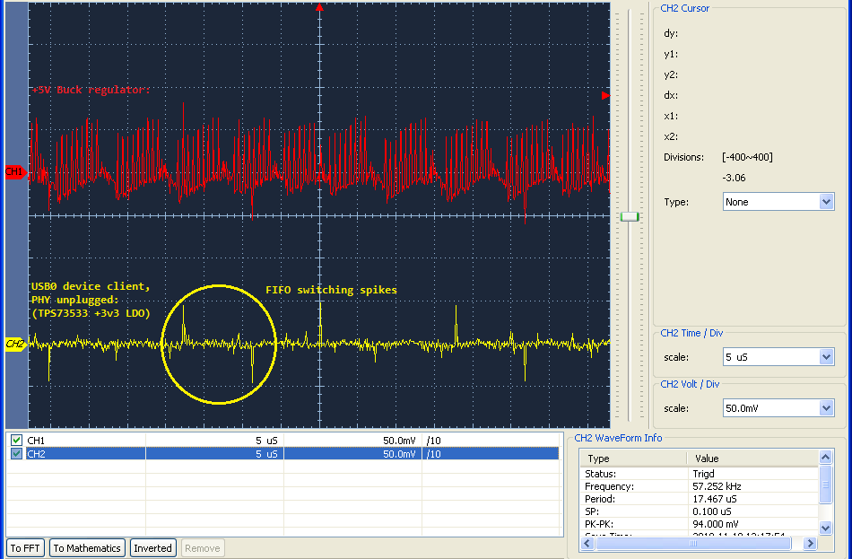
The 5V buck regulator custom PCB adjusts to current demand MCU upon 3v3 LDO regulator >102mV ripple. Added ferrite beads or even larger bypass caps LDO (TPS73533) fail to reduce >DC ripple of both peripherals.

Has any remedy been discovered or answer as to why EMAC0 current increases just plugging cable, closing loop? Likewise why USB0 bulk device endpoint client simply being launched produce >90mV switching spikes upon 3v3 LDO of either PCB? USB0 OTG port switching spikes (>90mV) seem to be data bus related noise yet are unacceptable ripple levels on either PCB.     

  • If the ripple in your custom board is <16mV then it is within the limit of the chip power supply operating range.
    The table 27.23 shows max of about 105mA at 25C Nominal with EMAC/PHY turned on which is close to your measurement.
  • Hi Charles,

    Charles Tsai said:
    If the ripple in your custom board is <16mV then it is within the limit of the chip power supply operating range.

    Perhaps you meant to say <17mA current draw. Expected peripheral load current EMAC0 is listed table 27.34, ALL peripherals enabled (105.3mA). With differential pair PHY (closed loop) DC ripple gets >50mV PP. The configuration of EMAC0 pulse XFMR closed loop artifact of increasing load current 25mA (EVM) and 17mA (custom PCB) is not listed in datasheet table 27.34. Listed values are for ALL peripherals maximum load current under RUN mode condition! 

    Something is wrong on both the EVM and our custom PCB. Seemingly Pulse XFRM secondary (client side) excessively loads primary (target) PHY differential pair! It would also seem no engineer ever tested MCU load current JP2 on EVM remains consistent as the PHY differential pair loop was close/open. Most never think testing JP3 load current increases >17mA simply PHY plugging cable. Perhaps Pulse XFMR rep might have some information why PHY current increase occurs beyond Table 27.34 limits? 

    Again table 27.34 states (ALL) peripherals enabled, we only have a few peripherals enabled. Increase of MCU load current simply closing PHY differential pair loop has not been listed as an expected artifact. Let alone the PP ripple on 3v3 supply >50mV result from 17-25mA load increase when closing the PHY loop!

  • Hi Charles,

    Researching VDD/VDDA guidelines it seems the two 1uf caps changed 4.7uf for Pulse XFMR 3v3 bias did not reduce the USB0 data switching spikes shown in above capture. Design guide suggest place bulk cap near MCU and combined VDD/VDDA is between 2-22uf can be place on VDD decoupling, text below.  

    Do we include the Pulse XFMR bias caps values part of 22uf or Bulk cap? The 3v3 rail layout: TPS73533 +3v3 LDO 3.3uf cap first provides VDD rail, four bypass 0.1uf caps, one on each side of MCU 0.4uf total. Oddly MCU area of the PCB in my opinion has solid power and ground planes. Yet scope capture above argues point as ripple increases EMAC0 PHY loop is closed, adds >50mV ripple on 3v3 LDO regulator.  

    The design guide text is vague, do we replace VDD 0.1uf caps with larger value capacitance or parallel existing 0.1uf? Is paralleling via two VDD cap values best practice to reduce high speed USB/PHY data switching spikes? 

    3.4.3 Decoupling Capacitors

    Ideally, Tiva™ C Series microcontrollers should have one decoupling capacitor in close proximity to each power-supply pin. Decoupling capacitors are typically 0.1 μF in value and should be accompanied by a bulk capacitor near the microcontroller. The combined VDD and VDDA bulk capacitance of the microcontroller is typically between 2 μF and 22 μF, with values on the upper end of that range providing measurable ripple reduction in some applications, especially if the circuit board does not have solid power and ground planes. Bulk capacitance is particularly important if the microcontroller is connected to high speed interfaces or must source significant GPIO current (that is, greater than 4mA) on more than a few pins.


  • Adding Pulse XFMR 3v3 bias caps (2x 4.7uf) with MCU bulk caps plus two 3.3uf in parallel 0.1uf VDD pins, bulk MCU capacitance <21uf.
    Reduced 3v3 ripple (38mV) with 92mA load, closed PHY/USB loops. The 3v3 rail trace to VDD pins lastly feeds the Pulse XFMR below the MCU VDD rail caps.

    Also increased 3.3uf to 4.7uf input TPS73533 being proximity to +5v buck regulator <6mm. Increasing to 4.7uf really lowered the impedance on TPS73533 input, still did not reduce USB0 switching spikes frequency. Perhaps the computer USB port is causing high speed data spikes, not the target?
  • All bets are off when it comes to lowering EPHY/USB  ripple <32mV and required additional 3.5uf cap placed on LDO regulator to reduce USB0 spikes, not entirely arresting them. TPS73533 datasheet warns greater capacitance 3v3 ripple transient response longer duration. It seems the added capacitance lowered the impedance on MCU 3v3 rail traces along with to parallel 3.3uf/0.1uf on two sides of MCU.

    Additional 3.5uf (4.7uf) to 3v3 LDO bulk cap + VDD pins 6.6uf total capacitance does not arrested USB0 bulk device client sudden disconnects. Seemingly USB0 device client disconnects upon any VDD transient glitch thus disrupting the differential pair. Later added10-20n parallel with bulk cap of LDO as 3v3 TVS and reducing DC ripple had no effect to stop VDD glitches.

    The 17-20mA additional current draw from EPHY differential loop closing has not been explained via Tables 27.63/64. Seemingly additional 3v3 current loading indicates Pulse transformer BIAS thus causes >DC ripple is not typical or expected EPHY behavior! 

  • HI Charles,

    Have you tested EPHY loop closing current loads 3v3 LDO DC ripple JP2 of EVM? Any conclusion as to why EPHY idle current (72mA) rises >92mA DC ripple >40mV as Pulse XFMR diff pair loop closes? USB0 client loop closure now adds little to no DC ripple other than data glitches shown is first capture, blending below capture. The DC ripple similarities between EVM and our custom PCB prove EPHY being a major contributor in both.  

    Below capture taken custom PCB after adding 3.3uf caps two sides of MCU VDD pins parallel (3.3uf, 4.7uf) 3v3 LDO. Following TM4C129 design guide Pulse XFMR 3v3 bias caps were updated 4.7uf (<10uf) made little difference to DC ripple >50mV (92mA) VDD rail.  

    Seemingly C18, C22, (0 .1uf) EVM are not proper value either to reduce U5 (TPS73733) DC ripple <17mV. What is going on in HW to cause ripple values current loading outside table 27.23 Run time current consumption? What values C18, C22 would be better to arrest glitches riding on DC ripple <40mV? It would seem the EVM also has NRC value C19 (0.1uf) and 10n is suggested max value TPS73733 datasheet. Forum had little info late 2015 of DC ripple JP3 and no one was aware EPHY loop closure a contributor. Seemingly >32mV  DC ripple can also be reduced by lowering Pulse XFMR current consumption in EPHY closed loop. Lately finding 100n bypass is not always the best choice in transient response and certain cap values may actually sustain undesired artifacts.