


Part Number: TM4C1294KCPDT
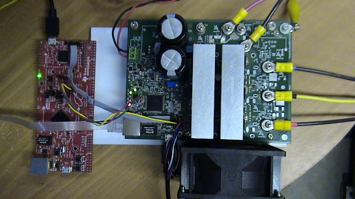
It is clear that EMI entering via ADC channels is attacking USB, EMACK and GPTM edge counts. Oddly 3" to 6" connect wires X11 header to DC inverter masked over EMI issue, a custom PCB engineer is left to contend with. The proximity of MCU to EMI entering AINx channels is verified somehow enters VDD/LDO or the AHB and attack certain peripherals. No matter the bulk capacitance added on VDD pins there is no improvement to reduce inductive EMI.
The remedy to avert SCR latch up of USB0, PHY0 includes changing decoupling capacitance values on AINx channels 200pf reduced to 100pf or less. How is allowing more EMI to enter MCU stopping PHY latch up but then immediately crashes USB0 and effects GPTM edge counts? The EVM X11 Booster pack headers and OTG port are both immune to very same EMI source. We do not have the proper laboratory environment to uncover what the difference is.
Has TI considered updating TM4C1294 design guide as how to protect MCU exposed proximity to EMI source such as a DC inverter? Again the EVM X11, Booster Pack headers misleads engineers TM4C1294 MCU is mostly immune to EMI as OTG, PHY, GPTM edge counters are not effected by the very same EMI source.

