Hello everyone, I am using the TMS570LS1227's two-Channel SCI interface to send data at the same time. The SCI/LIN transmission data is normal, but another single SCI interface is not sent properly, and its TX pin is always low! Anyone who can answer this question? thank you very much!
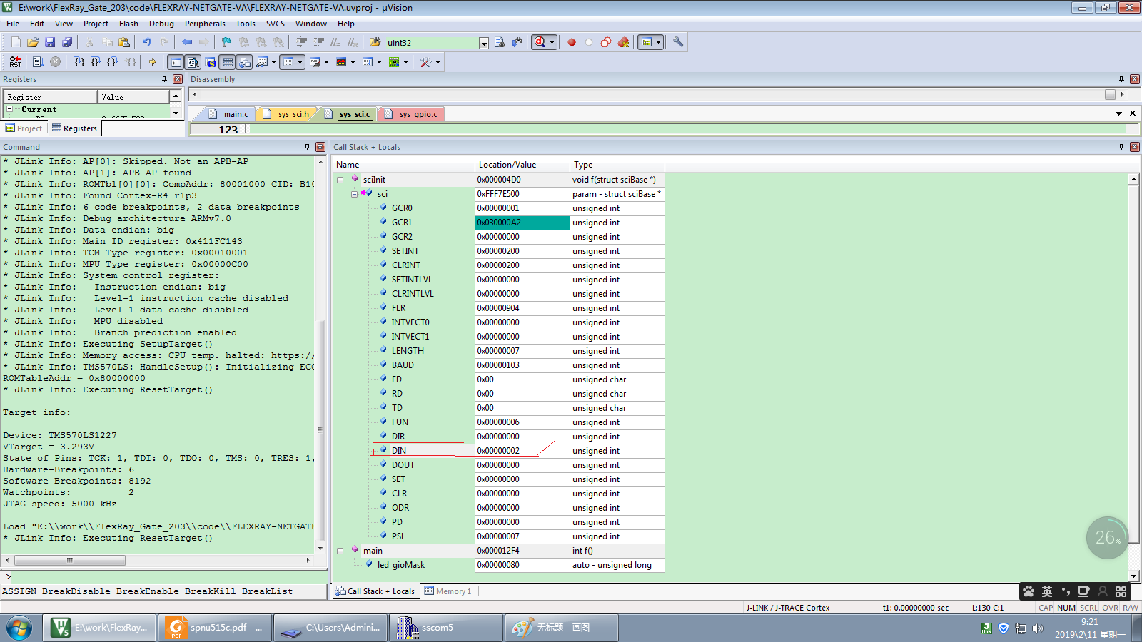
The following is my code and the contents of the relevant registers after initialization is completed.
void sciInit(void)
{
/** @b intalise @b SCI1 */
/** - bring SCI out of reset */
sciREG1->GCR0 = 1U;
/** - Disable all interrupts */
sciREG1->CLRINT = 0xFFFFFFFF;
sciREG1->CLRINTLVL = 0xFFFFFFFF;
/** - global control 1 */
sciREG1->GCR1 = (1 << 25) /* enable transmit */
| (1 << 24) /* enable receive */
| (1 << 5) /* internal clock (device has no clock pin) */
| (0 << 4) /* number of stop bits */
| (0 << 3) /* even parity, otherwise odd */
| (0 << 2) /* enable parity */
| (1 << 1) /* asynchronous timing mode */
| (0 << 0);
sciREG1->GCR1 = 0x03000022;
/** - set baudrate */
sciREG1->BAUD = 259; /* 19.2KHz, baudrate */
/** - tranmision length */
sciREG1->LENGTH = 7; /* length is 7+1 */
/** - set SCI pins functional mode */
sciREG1->FUN = (1 << 2) /* tx pin */
| (1 << 1) /* rx pin */
| (0); /* clk pin */
/** - set SCI pins default output value */
sciREG1->DOUT = (0 << 2) /* tx pin */
| (0 << 1) /* rx pin */
| (0); /* clk pin */
/** - set SCI pins output direction */
sciREG1->DIR = (0 << 2) /* tx pin */
| (0 << 1) /* rx pin */
| (0); /* clk pin */
/** - set SCI pins open drain enable */
sciREG1->ODR = (0 << 2) /* tx pin */
| (0 << 1) /* rx pin */
| (0); /* clk pin */
/** - set SCI pins pullup/pulldown enable */
sciREG1->PD = (0 << 2) /* tx pin */
| (0 << 1) /* rx pin */
| (0); /* clk pin */
/** - set SCI pins pullup/pulldown select */
sciREG1->PSL = (1 << 2) /* tx pin */
| (1 << 1) /* rx pin */
| (1); /* clk pin */
/** - set interrupt level */
sciREG1->SETINTLVL = (0 << 26) /* Framing error */
| (0 << 25) /* Overrun error */
| (0 << 24) /* Pariry error */
| (0 << 9) /* Receive */
| (0 << 8) /* Transmit */
| (0 << 1) /* Wakeup */
| (0); /* Break detect */
/** - set interrupt enable */
sciREG1->SETINT = (0 << 26) /* Framing error */
| (0 << 25) /* Overrun error */
| (0 << 24) /* Pariry error */
| (1 << 9) /* Receive */
| (0 << 1) /* Wakeup */
| (0); /* Break detect */
/** - set interrupt enable */
sciREG1->CLRINT = (0 << 26) /* Framing error */
| (0 << 25) /* Overrun error */
| (0 << 24) /* Pariry error */
| (0 << 9) /* Receive */
| (0 << 1) /* Wakeup */
| (0); /* Break detect */
/** - inialise global transfer variables */
// g_sciTransfer[0].mode = 0 << 8;
// g_sciTransfer[0].length = 0;
/** - Finaly start SCI1 */
sciREG1->GCR1 |= 0x80;
/** @b intalise @b SCI2 */
/** - bring SCI out of reset */
sciREG2->GCR0 = 1U;
/** - Disable all interrupts */
sciREG2->CLRINT = 0xFFFFFFFF;
sciREG2->CLRINTLVL = 0xFFFFFFFF;
tmp_reg = sciREG2->DIN;
/** - global control 1 */
sciREG2->GCR1 = (1 << 25) /* enable transmit */
| (1 << 24) /* enable receive */
| (1 << 5) /* internal clock (device has no clock pin) */
| (0 << 4) /* number of stop bits */
| (0 << 3) /* even parity, otherwise odd */
| (0 << 2) /* enable parity */
| (1 << 1) /* asynchronous timing mode */
| (0 << 0);
sciREG2->GCR1 = 0x03000022;
/** - set baudrate */
sciREG2->BAUD = 259; /* 19.2KHz, baudrate */
/** - tranmision length */
sciREG2->LENGTH = 7; /* length is 7+1 */
/** - set SCI pins functional mode */
sciREG2->FUN = (1 << 2) /* tx pin */
| (1 << 1) /* rx pin */
| (0); /* clk pin */
/** - set SCI pins default output value */
sciREG2->DOUT = (0 << 2) /* tx pin */
| (0 << 1) /* rx pin */
| (0); /* clk pin */
/** - set SCI pins output direction */
sciREG2->DIR = (0 << 2) /* tx pin */
| (0 << 1) /* rx pin */
| (0); /* clk pin */
/** - set SCI pins open drain enable */
sciREG2->ODR = (0 << 2) /* tx pin */
| (0 << 1) /* rx pin */
| (0); /* clk pin */
/** - set SCI pins pullup/pulldown enable */
sciREG2->PD = (0 << 2) /* tx pin */
| (0 << 1) /* rx pin */
| (0); /* clk pin */
/** - set SCI pins pullup/pulldown select */
sciREG2->PSL = (1 << 2) /* tx pin */
| (1 << 1) /* rx pin */
| (1); /* clk pin */
/** - set interrupt level */
sciREG2->SETINTLVL = (0 << 26) /* Framing error */
| (0 << 25) /* Overrun error */
| (0 << 24) /* Pariry error */
| (0 << 9) /* Receive */
| (0 << 8) /* Transmit */
| (0 << 1) /* Wakeup */
| (0); /* Break detect */
/** - set interrupt enable */
sciREG2->SETINT = (0 << 26) /* Framing error */
| (0 << 25) /* Overrun error */
| (0 << 24) /* Pariry error */
| (1 << 9) /* Receive */
| (0 << 1) /* Wakeup */
| (0); /* Break detect */
/** - set interrupt enable */
sciREG2->CLRINT = (0 << 26) /* Framing error */
| (0 << 25) /* Overrun error */
| (0 << 24) /* Pariry error */
| (0 << 9) /* Receive */
| (0 << 1) /* Wakeup */
| (0); /* Break detect */
/** - inialise global transfer variables */
// g_sciTransfer[0].mode = 0 << 8;
// g_sciTransfer[0].length = 0;
tmp_reg = sciREG2->DIN;
/** - Finaly start SCI2 */
sciREG2->GCR1 |= 0x80;
}