


Posting this here in the hopes that it helps someone else. After spending a few days trying to figure out why SPI clock polarity 0 and phase 0, which I would call Mode 0, didn't work as expected.
Here's an example of what most people expect Mode 0 (CPOL=0, CPHA=0) to look like, from the TI CC26x0 TRM:

In this timing diagram, SSIn_Rx might more appropriately be called MISO, and SSIn_Tx would be called MOSI.
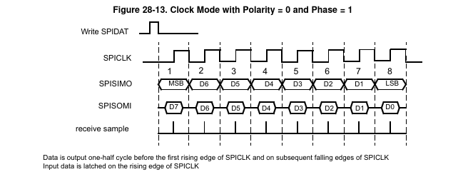
It seems that the TMS570 SPI implementation (mibSPI) has a strange idea of what phase 0 should be. Here's the same diagram from the TMS570LC4357:

Obviously, this won't work very reliably when talking to a "standard" Mode 0 SPI peripheral. What you might want is to change phase to a 1:
Hope that helps someone!
