This thread has been locked.

If you have a related question, please click the "Ask a related question" button in the top right corner. The newly created question will be automatically linked to this question.

TM4C123GH6PM: ADC using Differential mode is NOISY

Part Number: TM4C123GH6PM

Hey,


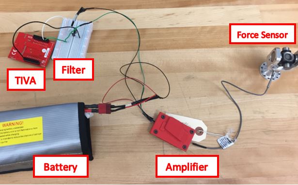
I'm trying to use the ADC to read the voltage of a force sensor I'm calibrating. The Force sensor outputs positive voltage for one direction and negative voltage for the other. I've setup my code to test single ended mode and differential mode, but I'm having issues using the differential mode. The output is very noisy. I attached an oscilloscope to observe the noise from the sensor.


I saw a consistent noise of ~20mV, but the output of the ADC is showing somewhere around ~150-200 mV of noise. The output is also really weird. The noise will only really sit on top of the expected value, it never goes below it. More on that below. Here is my code.


extern void ADCConfig_Diff(){

       SysCtlPeripheralEnable(SYSCTL_PERIPH_ADC0);


       //

       // For this example ADC0 is used with AIN0/1 on port E7/E6.

       // The actual port and pins used may be different on your part, consult

       // the data sheet for more information. GPIO port E needs to be enabled

       // so these pins can be used.

       // TODO: change this to whichever GPIO port you are using.

       //

       SysCtlPeripheralEnable(SYSCTL_PERIPH_GPIOE);


       //

       // Select the analog ADC function for these pins.

       // Consult the data sheet to see which functions are allocated per pin.

       // TODO: change this to select the port/pin you are using.

      //

       GPIOPinTypeADC(GPIO_PORTE_BASE, GPIO_PIN_3 | GPIO_PIN_2);


       //

       // Enable sample sequence 3 with a processor signal trigger. Sequence 3

       // will do a single sample when the processor sends a signal to start the

       // conversion. Each ADC module has 4 programmable sequences, sequence 0

       // to sequence 3. This example is arbitrarily using sequence 3.

       //

       ADCSequenceConfigure(ADC0_BASE, 3, ADC_TRIGGER_PROCESSOR, 0);


       //

       // Configure step 0 on sequence 3. Sample channel 0 (ADC_CTL_CH0) in

       // differential mode (ADC_CTL_D) and configure the interrupt flag

       // (ADC_CTL_IE) to be set when the sample is done. Tell the ADC logic

       // that this is the last conversion on sequence 3 (ADC_CTL_END). Sequence

       // 3 has only one programmable step. Sequence 1 and 2 have 4 steps, and

       // sequence 0 has 8 programmable steps. Since we are only doing a single

       // conversion using sequence 3 we will only configure step 0.   For more

       // information on the ADC sequences and steps, refer to the datasheet.

       //

       ADCSequenceStepConfigure(ADC0_BASE, 3, 0, ADC_CTL_D | ADC_CTL_CH0 |

                               ADC_CTL_IE | ADC_CTL_END);


       //

       // Since sample sequence 3 is now configured, it must be enabled.

       //

       ADCSequenceEnable(ADC0_BASE, 3);


       //

       // Clear the interrupt status flag. This is done to make sure the

       // interrupt flag is cleared before we sample.

       //

       ADCIntClear(ADC0_BASE, 3);

}


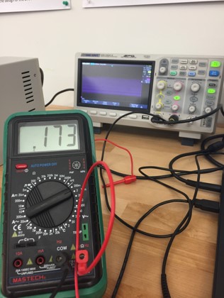
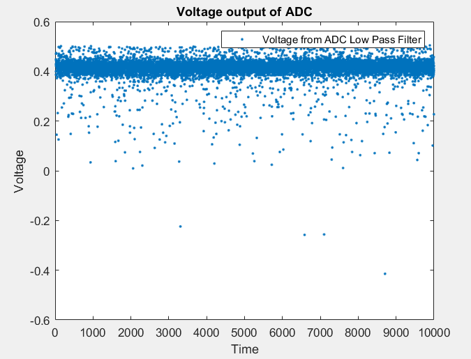
Here is the curve. A multimeter showed an output from the force sensor to be 0.384 V. Ignore the legend, it is the unfiltered value.

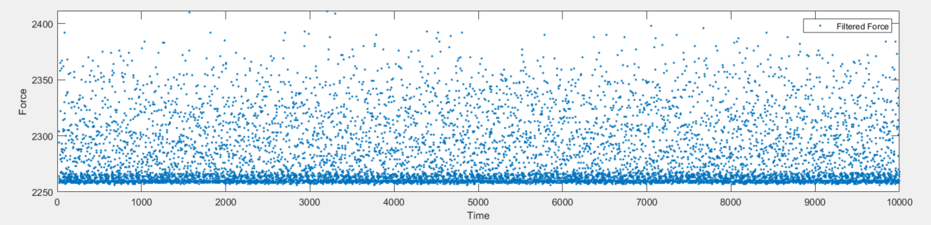
A value of 0.384 should approximately return 2260, which there is an unmistakable dark line to show consistency, but then there is a lot of extra points above this. At an adc_val of 2350, this is roughly 150 mV above the value, but while watching the oscilloscope, there was never any noise near this range. 

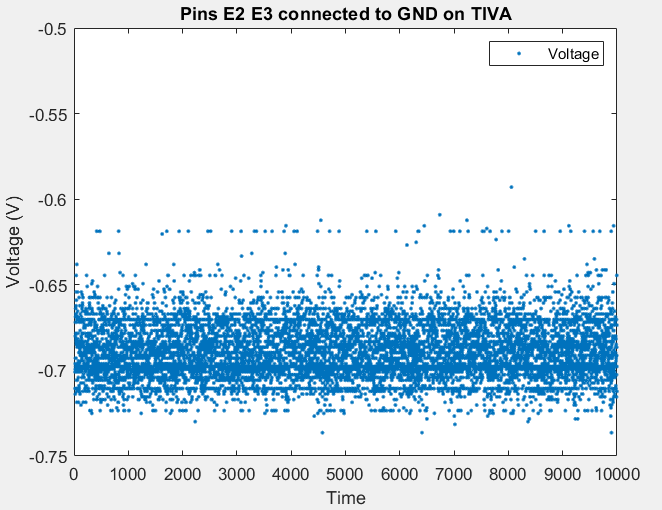
Also, here is the response of the same sensor at a similar voltage using the single-ended option.

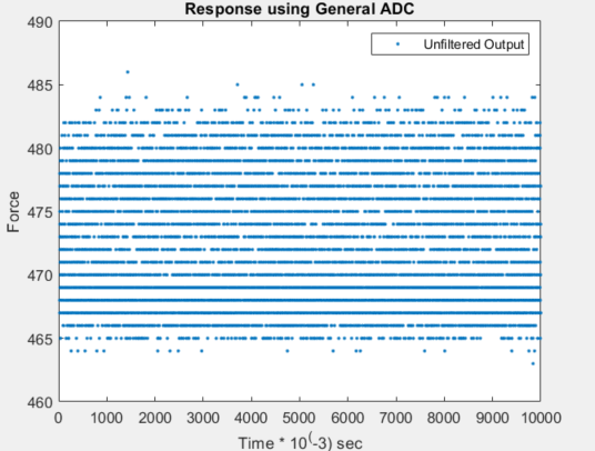
This value shows so much more accurate results, that you can visually see the sensor resolution.


Any help would be appreciated. Thanks!


  • First of all, do not connect a negative voltage to an ADC input, even in differential mode. The negative voltage on the ADC input pin will turn on an ESD protection diode and pull the internal analog ground of the ADC below GND which will cause the resulting ADC result to be wrong and high (or it might damage the device). Is your sensor really outputting a differential signal, or a bipolar signal? Other than that, make sure your ADC sample time is sufficient for the source impedance. Remember that noise on VDDA, GNDA or either of the differential inputs will affect your results.
  • The signal outputs as a unipolar signal with a data Out pin and GND. I essentially tried to use this as a bipolar wave where the GND pin of the sensor went into Pin E2 & the Data out from the sensor was put into the E3 pin on the TIVA. When I scoped the signal from the sensor, I only saw ~20 mV of suspected noise.

    Do you think that using Sequencer 0 instead of Sequencer 3 would give better results? 

  • I scoped the E2 and E3 pins on the ADC and found noise consistently at 0.173 V!

    Is there any way to remove this noise? This comes directly from the difference between the two pins. That amount of difference is very significant to me.

  • If there is noise in the signal, then the ADC conversion results will reflect that noise. If the noise is random, using averaging or a low pass filter will help. If the noise is not random (mostly high, or mostly low) either of those methods will see an offset in the results.
  • I've tried putting it on different pins (E0 & E1), and I connected the differential output a power supply at 0.5 V. Even stranger, I connected pins E2 and E3 directly to the ground pins on the TIVA.

    This is connected to an input voltage of 0.5 V. The y-axis scale is measured in Volts. The noise is quite consistent even when I'm using a low pass filter with a cutoff frequency of 10 Hz. When I shorted the outputs together on the ADC, I got a very constant reading of 0 V. But when I connected both outputs to the signal ground on the TIVA I got a pretty bizarre response.

    I'm really lost with this, because I don't understand why the output would look so noisy and the two different pins are connected to the exact same voltage. Why would the ADC see a consistent difference of -0.7V?? 

  • If you see the same noise when doing single ended conversions, then the noise is probably on VDDA with respect to GNDA. If the single ended conversion is clean, you might have a loop area in the connection to the two ADIN channels that might be picking up induced noise.
  • I have no issues doing single ended conversion, but I'm not quite sure what you mean by loop areas. The last graph I posted is where both pins are connected to the exact same GND pin on the TIVA. I'm not quite sure how the voltage could be different because they're connected to the same GND and nothing else.
  • By loop area I am asking about how the two ADIN pins are connected to that ground point. For example, if you used a launchpad and connected the two ADIN pins to a ground pin using jumper wires, the area circumscribed by the path from the ADIN pad, to the header pin though the first wire, through the second wire and from the second header pin back to the second ADIN pin creates a loop antenna. A magnetic field that passes through the loop antenna induces a voltage difference between the two terminals. The bigger the loop, the more magnetic field captured and the bigger the voltage difference. On the other hand, a trace on a PCB that connects two ADIN pin together and then tees out to connect to the nearest ground pin would create a very small loop.
  • I've test a variety of theories in the past few days. It seems like a significant portion of noise comes from the ADC towards voltage values of 0 V. I've tried this on 4 different sets of pins and I'm still getting the same response. The ADC output gets extremely noisy below 0.5 V. That's why when I was doing my calibration at a voltage reading of 0.384 V that the output was extremely noisy. Has anyone else ever experienced this?

    The ADC was plugged into a DC power supply were the voltage was lowered by hand to see the response. This response is the same regardless of the use of an analog low pass filter.

  • I was able to confirm that the noise I'm seeing is coming from the amplifier I'm using. I used a small 1.5 V battery attached to a potentiometer to adjust the voltage the ADC was seeing. The output was extremely clean, no noise. Many of issues I saw previously were caused by various electronic devices attached adding noise (DMM, Oscope, even the power input to my computer).

    My last issue in eliminating the 60 Hz input noise coming from my amplifier input. For some reason, the ADC has issues within a range of 0.5 V to -0.5 V, but outside of this range the waveform looks extremely clean.

    I want to use some sort of low pass filters which won't have issues with the polarity transitioning from negative to positive. Any recommendations on a good one?
  • The ADC inputs to the TM4C are not allowed to go below the ground of the TM4C. There are ESD protection diodes that will clamp the input signal.
  • I made a mistake earlier when describing the signal. It is bipolar. I've been able to get my noise lowered significantly by using decoupling capacitors to the TM4C's GND. The difference between the two inputs is very clean, but I'm worried that the input voltages might go above 3.3V. How does the TM4C make sure that the input voltages are below 3.3V since I'm using my GND as an input pin?
  • If I understand you correctly, your signal is bipolar with respect to the ground of the sensor, but you offset the signal so that it is unipolar with respect to the ground of the TM4C?

    The input signals are diode clamped if they go below ground and are Zener diode clamped on the positive side at 5V above ground. However, for accurate results both the inputs (Vin_even and Vin_odd) must be in the range of VREFN to VREFP (usually 0V to 3.3V). See page 811 of the datasheet for more details.  

  • The problem I'm having is that my current setup works because the TIVA GND and the sensor GND are not connected. I've used decoupling capacitors to clean the DATA and GND response from the sensor. The response is very good, but if I have no way to manage the two GNDs, then there's no way of knowing when Vin_even and Vin_odd are within the VREFN and VREFP range. I've tried connecting the TIVA GND and the sensor GND, but everytime I do that the TIVA will read a higher voltage than what I read on the DMM and then its voltage value will not change when I apply force to the force sensor even though I'm watching the voltage value change on the DMM.

    Then here's a bit on the circuit connections.

    The two system GNDs float relative to eachother. Whenever I connect the TIVA gnd and the sensor GND I get very bizarre responses. I tried to rectify the negative portion of the wave to become the input of the TIVA as well as the data input and when using the DMM I'll read 0.35V, but the TIVA will read 0.6 V. I think that the problem I'm having at this point is trying to figure out why the two systems act so different once their GNDs are connected. 

  • OK, I understand what you are doing. It is usually bad design practice to have an input signal with no common ground reference. Here is a short article I found on the internet (not from TI) that describes converting a bipolar signal into a unipolar signal for input to an ADC.
    masteringelectronicsdesign.com/.../