This thread has been locked.

If you have a related question, please click the "Ask a related question" button in the top right corner. The newly created question will be automatically linked to this question.

GPTM0 CCP PL4 into PL5 loads

Guru 55913 points
Part Number: TM4C1294KCPDT
Other Parts Discussed in Thread: EK-TM4C1294XL

Relative to same issue of edge counts unidentified internal noise source; Scenario GPTM0A CCP0 configured 20Khz PWM and GPTM0B CCP1 input edge counts, wire PL4 into PL5 with WPU oddly drags down 4mA PL4 near 2v. Adding Schottky in series PL4 to PL5 produces whisker like 20Khz pulses riding on 3v. Otherwise PL4 (CCP1) counts 49-200Hz edges from external open collector Taco source without issues until other GPTM are later being enabled, GPTM1A and GPTM4A each configured as Oneshot timers, 1A with interrupt vector and 4A as an ADC trigger source to ADC0 SS2. Both GPTM0A/B use alternate PIOSC clock source and have no match events configured lower than 0xD3. 

How could PL5 CCP0 input to PL4 WPU pull down the signal? DMM check PL5 has typical 1.7v drop and 6 Megohms to ground. Why would the open collector on PL5 not pull down the signal even though is much slower rate than PL4 20Khz? It seems like PL5 is acting like an bidirectional GPIO port when PL4 PWM signal is input to it.
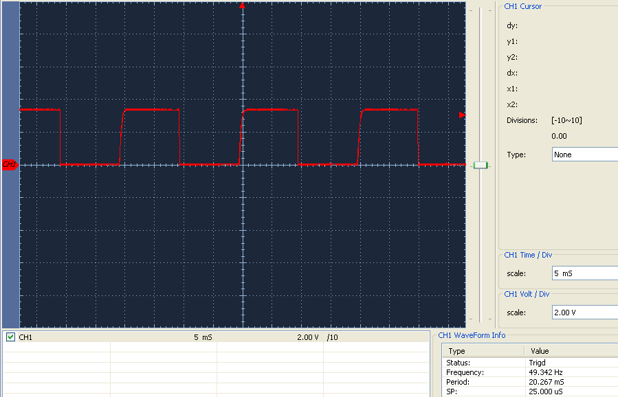
20Khz CCP0 PWM PL4  

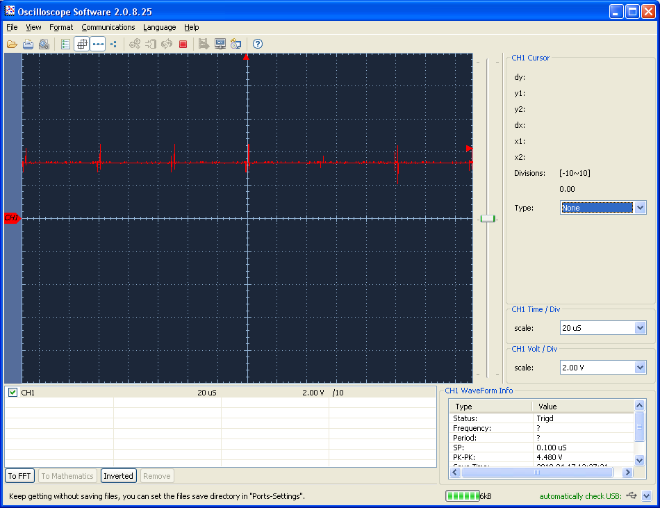
Open collector Taco source PL5 WPU:

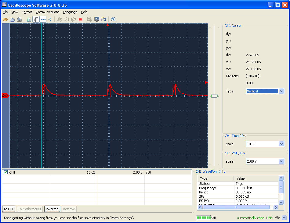
PL4 input to PL5 WPU without open collector signal above:


  • I suspect that the issue is noise from your motor control system that is injected into the TM4C1294. If the problem is not from your system, but inherent in the TM4C1294, then you should be able to reproduce this on a stand-alone EK-TM4C1294XL launchpad. If you can do that, then I can reproduce the problem and will be able to debug and resolve it.
  • Hi Bob,

    All but a motor is not even running under wrap test above, PL4 current path loads 4mA PWM drive of PL5.

    Seemingly loading should not occur on any MCU when configured PWM CCP mode and Edge counts on same GPTM half wide timer.  Oddly CCS debug shows PADs set above 2mA it just added 4mA bit sets and added 8mA where the SR control register was set for PWM0 generator pins. Anyone might think 4+8=12mA when only 8mA with faster slew rate was defined.  GPIOPadConfigSet() should first redact any previous current setting prior to changes but seemingly it does not do so. Otherwise seems harmless enough at first but perhaps more than one current setting per GPIO pin is a Boo Boo in the MUX logic?

    Tivaware GPIOPinTypeXXX() calls GPIOPadConfigSet() forcing a preset mA setting and calling GPIOPadConfigSet() again to change the previous value leaves the original MUX setting intact.

    Often designers don't require the default GPIOPadConfigSet() 2mA pin type setting especially when the Slew Rate register is later being called on specific GPIO pins. Datasheet text states I/O slew rate also increases with pins set for a higher milliamp drive strength. 

        // 20Khz PWM Duty PL4:TM0CCP0
        MAP_GPIOPinTypeTimer(GPIO_PORTL_AHB_BASE, GPIO_PIN_4);
        MAP_GPIOPadConfigSet(GPIO_PORTL_AHB_BASE, GPIO_PIN_4,
                             GPIO_STRENGTH_4MA, GPIO_PIN_TYPE_STD);
        MAP_GPIOPinConfigure(GPIO_PL4_T0CCP0);
    
        // Taco input PL5:TM0CCP1
        MAP_GPIOPinTypeTimer(GPIO_PORTL_AHB_BASE, GPIO_PIN_5);
        MAP_GPIOPadConfigSet(GPIO_PORTL_AHB_BASE, GPIO_PIN_5,
                             GPIO_STRENGTH_4MA, GPIO_PIN_TYPE_STD_WPU);
        MAP_GPIOPinConfigure(GPIO_PL5_T0CCP1);


  • The GPIO current control registers have a few aspects that differ based on the last sentence below. The PL5 loading was caused by 22nf decoupling cap and 100 ohm series PL4, the PWM signal was rolling off in the minimal duty cycle. There should have been roughly 400mV drop from 100 ohms which limits high 2.9v PWM signal to 29mA. It seems there is not 4mA being delivered on PL4 even as PAD was set to 4mA in debug register view and 2mA bits are clear. The 22nf/25v ceramic cap was out of tolerance but not shorted. Removing 22n was the cure to stop the excessive roll off only when PL4 PWM signal was input to PL5 edge count timer. 
     
    10.3.5.1 Extended Drive Enable
    The GPIO Peripheral Configuration (GPIOPC) register controls the extended drive modes of the
    GPIO. When the EDE bit in GPIO Peripheral Properties (GPIOPP) register is set and the EDMn bit
    field for a GPIO pin is non-zero in the GPIOPC register, the GPIODRnR registers do not drive their
    default value, but instead output an incremental drive strength, which has an additive effect. This
    allows for more drive strength possibilities. When the EDE bit is set and the EDMn bit field is non-zero,
    the 2 mA driver is always enabled. Any bits enabled in the GPIODR4R register for a pin with a
    non-zero EDMn value, add an additional 2 mA. Any bits set in the GPIODR8R add an extra 4 mA of
    drive. The GPIODR12R register is only valid when the EDMn value is 0x3. For this encoding, setting
    a bit in the GPIODR12R register adds 4 mA of drive to the already existing 8 mA, for a 12 mA drive
    strength. To attain a 10-mA drive strength, the pin's GPIODR12R and GPIODR8R register should
    be enabled; this would result in the addition of two, 4-mA current drivers to the already enabled
    2-mA driver. The table below shows the drive capability options. If EDMn is 0x00, then the GPIODR2R,
    GPIODR4R, and GPIODR8R function as stated in their default register description

    Register 12: GPIO 4-mA Drive Select (GPIODR4R), offset 0x504
    The GPIODR4R register is the 4-mA drive control register. Each GPIO signal in the port can be
    individually configured without affecting the other pads. When setting the DRV4 bit for a GPIO signal,
    the corresponding DRV2 bit in the GPIODR2R register and DRV8 bit in the GPIODR8R register are
    automatically cleared by hardware.

    Only cleared by hardware if the EDMn bits are non-zero for the port in the GPIOPC register!!

  • Otherwise setting the PWM duty cycle to 50% also reduced loading of PL5 20KHz signal into PL4 input, even with 22nf remaining in the circuit.

  • BP101 said:
    There should have been roughly 400mV drop from 100 ohms which limits high 2.9v PWM signal to 29mA. It seems there is not 4mA being delivered on PL4 even as PAD was set to 4mA

    BP101,

    I don't understand this statement. If you are trying to drive a 100 Ohm resistor in series with a 22nF capacitor, the initial current would be 3.3V/100 Ohms or 33mA. That way exceeds the 4mA minimum drive current. You should expect to see an voltage curve increase as the 22nF capacitor charges. Perhaps a simple circuit diagram would help me understand what you are trying to say. The scope picture you provided does not have a voltage or time scale so it did not help.

  • Bob Crosby said:
    I don't understand this statement. If you are trying to drive a 100 Ohm resistor in series with a 22nF capacitor, the initial current would be 3.3V/100 Ohms or 33mA

    I always use I=E/R to limit the pin current to not exceed the resistors ohmic value, using Ohms law sets maximum current, not the minimum. Oddly the external open collector drive into PL5 input had no issue with 22n cap but driving PL5 from PL4 set to 4mA fails. This seems to prove PL4 being set 4mA drive strength is not producing 4mA. Again PL5 being limited to 29mA (100Ohm) of a GPIO pin out high level, not 3v3 DC supply. The maximum drop across 100ohm at 4mA drive strength and 2.9V logic high gets 400mV. Yet the 3rd scope capture shows nearly 1.2v drop, thus proves PL4 is not outputting 4mA even in the excessive 20Khz roll off.  

    The external open collector drive (5mA) into PL4 is now in series with 5.6K and triggering edge counts via the same 22n to ground. Have also replaced PL4 100ohm with 5.6K into 10K impedance (PWM) to control external noise from entering the GPIO pins. Oddly testing ferrites on the open collector PL4 produced voltage spikes above/below both MCU rails. Something is not right with that as ferrites (140mOhm / 1Kz@10Mhz) are supposed to reduce signal ringing not cause it. 

    Function: Frequency generator and PWM:

    /cfs-file/__key/communityserver-discussions-components-files/908/Fans-Orian-24v-circuit_5F00_diagrams.pdf    

  • This test to me indicates the CCP pin design can not produced our GPIO set drive strength (4mA) at certain duty and or frequency. The change in duty cycle from 1% to 50% @20Khz, last scope capture proves an drive strength errata for CCP pins.

    The second part of proof being PL5 PWM 1% duty 4mA drive strength (100Ω or 5.6K) into 10k external impedance does not load PL5,e.g 2nd capture 1st post.

  • BP101 said:
    This test to me indicates the CCP pin design can not produced our GPIO set drive strength (4mA) at certain duty and or frequency.

    I disagree. I think you are not taking into account the current that is needed to charge the 22nF capacitor and the time it will take for the voltage to rise. I have requested a diagram or schematic of what you have connected to PL4 and PL5 so that I might help you.

  • Bob Crosby said:
    have requested a diagram or schematic of what you have connected to PL4 and PL5 so that I might help you.

    Hi Bob,

    I don't see the relevance for a schematic for a simple wrap test PL4 into PL5 with a 100 ohms series resistor, 22n to ground decoupling PL4 near the pin.  The attached PDF being the simple intended configuration PL4 PWM drive and PL5 configured WPU and open collector edge counts via a single 32 bit GPTM, reveals issues in wrap testing. Will be testing onboard 24vdc buck regulator (fan power), an past tested dual 24vdc sources did not provide any better noise isolation for edge counter. Last ditch effort reduce 24v buck down to 12vdc and test new smaller 40mm fan with similar PWM tachometer drives.

    Bob Crosby said:
    I think you are not taking into account the current that is needed to charge the 22nF capacitor

    My view at this point is PL4 configured 4mA drive strength can not exactly drive 1% duty cycle thus PL4 is simply not producing 4mA, more like 2mA though debug indicates 4mA. Again last capture above post proves CCP drive strength 1% duty limitation exists and goes away @ 50% duty. Point of PDF being PL5 easily drives Orion fan PWM input (10K impedance) 1% duty via 100 ohm or 5.6k without loading. This occurs 518µA (5.6K) and does not require 4mA drive strength, so who'd be the wiser unless they did a wrap test? There is no reason that makes plausible sense other than full 4mA drive strength is not being set. The 100 ohm between PL4/PL5 limits source or sink currents up to 29mA (I=E/R), allowing 4mA load even @1% duty cycle. And again how is PL4 loading PL5 unless perhaps 2mA has been set as the PAD strength when 4mA is being indicated in debug register view?

    Another odd thing noticed launch pad LED's configured 2mA, 4mA, 8mA maintained same exact intensity, "green blinders of human eye sight." I reduced (gpio.c) GPIOPinTypeEthernet LED (8mA) drive strength to 2mA as default PAD current and/or for HW to auto clear 2mA bits when 4mA was set. Same goes for GPIOPadConfigSet() of other configured LED's, 2mA or 4mA have the same (sink current) intensity level via 330R in series to ground. If the current was regulated to 4mA lowered to 2mA there should be some noticeable shift in LED intensity. 

    Anyway CCP count/time inputs are not very friendly!

  • BP101,
    I asked for the schematic because I did not suspect that you are missing the obvious. It is the capacitor that is loading PL4, not that PL4 cannot provide the 4mA current and not that PL5 is loading the circuit. You have to treat a PWM as an AC circuit, not a DC circuit. Let's take the extreme example and treat PL4 as a constant current source of 4mA. The voltage on the capacitor is V = I * t / C (voltage = current x time / capacitance). Use a capacitance of 22nF, and a current of 4mA. A 1% duty cycle pulse of a 20KHz signal is 500nS. 4mA * 500nS / 22nF = 0.09V. The truth is that starting out PL4 is delivering more than 4mA, but it cannot deliver the 90mA that would be required for the voltage to reach Vih of PL5 before the PWM circuit switches PL4 low again and it starts draining the capacitor. Remove the capacitor from your circuit and then check the resulting PWM to verify that what I am saying is correct.
  • Bob Crosby said:
    A 1% duty cycle pulse of a 20KHz signal is 500nS. 4mA * 500nS / 22nF = 0.09V

    Yet the Orion PDF shows 5mA Max from Open collector frequency output and PL4 WPU and edge counts CCP1 is not being effected by 22n at 1% duty. I find your 1% duty math not to convincing in this scenario and lean more toward 2mA PAD strength is being produced even when 4mA has been set. The fan frequency output can not deliver 90mA drive strength to PL4 and 22n is not a problem @1% duty, only PL5.  

    Oddly input impedance @2mA (PL5 drive strength) increases to 1.45K and PL4 likewise push/pull input slew rate impedance follows, R=E/I given 2.9v high level. Where 2.9v/1450R=2mA, 2.9v/725R=4mA, 2.9v/363R=8mA pin drive slew rate impedance respectively.

    Again how to explain the EVM LED's (DC) does not change intensity GPIO PAD set 2mA or 8mA sinking LED via 330 ohm to ground? Noticed especially for Orange, Red LED's on the custom PCB. It seems GPIO mux PAD is not changing pin drive strength >2mA or is incorrectly coupled to the SL register for all drive strengths >2mA? 

  • I give you an exercise so that you may answer your own questions. Frist, what does TI mean by a 4mA output. We find the answer in table 27-7 of the datasheet. The output pin, in 4mA mode, can drive at least 4.0mA to a voltage of 2.4V.

    In other words, the pin should be able to drive a 600 Ohm resistor to 2.4V. Try it for yourself. You can use a standard 560 Ohm or 680 Ohm resistor if you don't have a 600 Ohm resistor handy. Drive it with the pin and measure the voltage. From that you can calculate the current that the pin is providing.

    To answer the LED question, here is a snippet from the EK-TM4C1294XL schematic showing that the LEDs are in series with a 330 Ohm resistor.

    By measuring the voltage at the positive end of the resistor, you can determine the current through the resistor. It is the same current through the LED. Also measure the voltage at the anode of the LED (same as measuring the voltage at the TM4C pin). Now compare these measurements with the pin configured for 2mA and then for 4mA. Finally, look at the LED datasheet for the luminosity at those currents. The LEDs are Everlight  19-217/G7C-AL1M2B/3T.

  • Hi Bob,

    If the current on the LED's is changing from 2, 4, 6mA luminosity change was not visually apparent for Lite-on LED's or the Everlights which have blinding green brilliance. The major problem with edge counts PL5 input ended up being ground pin related to the fans 24v power. Months ago moved GND pin from digital plane to the analog plane to quiet 3v3 supply of fan PWM noise.

    Past moving ground wire back to digital GND achieved no improvements for PL5 edge count stability. The only other thing I did differently today was change PL5 input from 4mA to 6mA, fan moved to digital GND and provided +22v from the on PCB buck regulator. The 22nf decoupling cap is still removed yet the PL5 input signal past appeared the same with the fans Taco signal. There is still minor stray in fans reported speed but nothing like it was previously all over the place.