This thread has been locked.

If you have a related question, please click the "Ask a related question" button in the top right corner. The newly created question will be automatically linked to this question.

Compiler/TM4C123GH6PZ: Not able to read external ADC Values using SPI communication

Part Number: TM4C123GH6PZ

Tool/software: TI C/C++ Compiler

Hi,

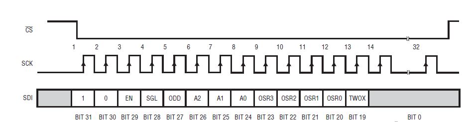
I am having issue while reading from an external ADC(part no. LTC2442) using SPI communication. I interface my tm4c123 board with external ADC LTC2442 using SPI. The ADC value what I am getting at the controller output is not matching with the input value at the ADC. I am using the 4 channels of the ADC. 

The below attached is the code I used for ADC read.

#include "main.h"
#include "LTC2442_ADC.h"


uint32_t ulDataRx[NUM_SSI_DATA] = {0x00,0x00};    // An array of 4 data bytes to be Rx
unsigned long ulindex; 

unsigned long ch0[NUM_SSI_DATA] ={0xB000,0x0000};   // B- 31-28 bit make dummy bit low/ 0 indicate 0000 channel 0 / '0'- 24-bit conversion result MSB first/Bits 4-0 are sub LSBs ignore this sublsb
unsigned long ch1[NUM_SSI_DATA] = {0xB100,0x0000};  //1 indicate 0001 channel 1 refer LTC2442 datasheet pages-11,12,13
unsigned long ch2[NUM_SSI_DATA] = {0xB800,0x0000};  //8 indicate 1000 channel 2
unsigned long ch3[NUM_SSI_DATA] = {0xB900,0x0000}; //9 indicate 1001 channel 3
unsigned int Raw_Value1 ;
unsigned int Raw_Value2;
unsigned long temp, temp1;

void LTC2442_SPI_config(void)
{
	ROM_SysCtlPeripheralEnable(SYSCTL_PERIPH_SSI0);
	while(!SysCtlPeripheralReady(SYSCTL_PERIPH_SSI0));
/*The SSI0eperipheral is on Port A and pins 2,3,4 and 5.*/
	ROM_SysCtlPeripheralEnable(SYSCTL_PERIPH_GPIOA);  
/*configure the port  pins for clock,chipselect,receiver,transmitter*/
    ROM_GPIOPinConfigure(LTC2442_SPI_CLK);
    ROM_GPIOPinConfigure(LTC2442_SPI_CS);
    ROM_GPIOPinConfigure(LTC2442_SPI_RX);
    ROM_GPIOPinConfigure(LTC2442_SPI_TX);
	  
/* Configure the pin for SSI*/	
	  ROM_GPIOPinTypeSSI(GPIO_PORTA_BASE, LTC2442_SPI_TX_PIN  | LTC2442_SPI_RX_PIN  | LTC2442_SPI_CS_PIN  | LTC2442_SPI_CLK_PIN);
/* Clock setting for SSI*/	
	  ROM_SSIConfigSetExpClk(SSI0_BASE, SysCtlClockGet(), SSI_FRF_MOTO_MODE_2, SSI_MODE_MASTER, 4000000, 16);
	  ROM_SSIEnable(SSI0_BASE);	
}
	
int LTC2442_ADC_OutputRead(unsigned int i)
{

	switch(i)
 {
	/* make cs pin to low after reading the adc data*/
	
		LTC2442_SPI_CS_LO;
  case 0:
  {
         for(ulindex = 0; ulindex < NUM_SSI_DATA; ulindex++)
        {
			   ROM_SSIDataPut(SSI0_BASE, ch0[ulindex]);
			     while(SSIBusy(SSI0_BASE)){}
			  }
				
				  for(ulindex = 0; ulindex < NUM_SSI_DATA; ulindex++)
        {
					ROM_SSIDataGet(SSI0_BASE, &ulDataRx[ulindex]);
				  while(SSIBusy(SSI0_BASE)){}
					SysDelay(1000);
				}
    }
   
   break;
  case 1:
  {   
		  
		   for(ulindex = 0; ulindex < NUM_SSI_DATA; ulindex++)
        {
			   ROM_SSIDataPut(SSI0_BASE, ch1[ulindex]);
			   while(SSIBusy(SSI0_BASE)){}
        }
				  for(ulindex = 0; ulindex < NUM_SSI_DATA; ulindex++)
        {
					ROM_SSIDataGet(SSI0_BASE, &ulDataRx[ulindex]);
				  while(SSIBusy(SSI0_BASE)){}
          SysDelay(1000);
				}
		    
  }
   break;
  case 2:
  {
           
		     for(ulindex = 0; ulindex < NUM_SSI_DATA; ulindex++)
        {
			   ROM_SSIDataPut(SSI0_BASE, ch2[ulindex]);
			   while(SSIBusy(SSI0_BASE)){}
 
         }
       for(ulindex = 0; ulindex < NUM_SSI_DATA; ulindex++)
        {
					ROM_SSIDataGet(SSI0_BASE, &ulDataRx[ulindex]);
				  while(SSIBusy(SSI0_BASE)){}
          SysDelay(1000);
				}

	}
   break;
  case 3:
  {
   
		    for(ulindex = 0; ulindex < NUM_SSI_DATA; ulindex++)
        {
			   ROM_SSIDataPut(SSI0_BASE, ch3[ulindex]);
			   while(SSIBusy(SSI0_BASE)){}
         
         }
				
				for(ulindex = 0; ulindex < NUM_SSI_DATA; ulindex++)
        {
					ROM_SSIDataGet(SSI0_BASE, &ulDataRx[ulindex]);
				  while(SSIBusy(SSI0_BASE)){}
					SysDelay(1000);	
 
				}
  }
   break;
  default:
   break;
  }
		/* make cs pin to high after reading the adc data*/

	LTC2442_SPI_CS_HI;
	Raw_Value1 = ulDataRx[0]; //MSB bit sending out of the ADC first 
	Raw_Value2 = ulDataRx[1];
	temp = Raw_Value1 << 16;     //shift the MSB bit left by 16 bit position/16bit MSB and then 16 bit LSB
	 
	temp1 =  temp | ulDataRx[1] ;
	
	temp1 &= 0x1FFFFFFF; /*force high three bits to zero*/
	temp1 >>= 5;   /*truncate lowest 5 bits/shift to right*/ 


	return temp1;
}

Please help me to solve the issue.

Thanks,

Alphy

  • Unfortunately to really help you requires knowledge of the LTC2442 and I am not an expert on my competitor's part. However, it looks to me like it requires the CS low during a 32 bit transfer with data valid after chip select and then clocked on the first rising edge of the clock (again verify this with the LTC datasheet or with their customer support). If that is the case, you need to manually toggle the CS. I see in your code that you configure the SSI FS pin, and you have a macro for CS_LO and CS_HI. Since I don't have the source of the macro, I cannot tell if this is what you are doing or not. (Getting a logic analyzer trace of the SSI pins usually helps a lot in this kind of debug.) Next, I think you need SSI_FRF_MOTO_MODE_0, not mode 3. I don't see in your code where you check that the EOC bit (SDO of the LTC when CS goes low) is low before you start the read. Finally, remember that each SSIDataPut() call does a read as well as a write. The next SSIDataGet() will read from the FIFO what was captured by the previous SSIDataPut(). When you use two SSIDataPut() calls to set the channel, the next two SSIDataGet() calls return the results from the previous channel, not the one you just selected. You may want to do one SSIDataPut() to set the channel (I think you can do that with a single 16 bit write). Then do one SSIDataGet() and throw away that dummy data. Then check for EOC to go low. then do two SSIDataPut() which will set the next channel to convert as well as initiate reading 32 bits from the first channel. Finally call SSIDataGet() twice to retrieve that information from the FIFO.
  • Hi sir, 

    I changed the code based on your previous reply and I am able to send the channel number correctly. But I am unable to get any output data from the ADC.

    The below mentioned are the correction I did based on your reply. 

    CS pin  low for the 32 bit data transfer. The FSS pin configuration I changed and so chip select is now working fine.verified with an oscilloscope.

    I am able to send the channel number correctly. Verified the output of clock and data input(SDI). It came perfectly. But I am unable to read data output(SDO).some noise signal is coming from the data output.

    In the debugger mode  some hex value came once and then getting Zero continuously.The hex value what I got is  invalid data.

    I am not able to take the snapshot from scope. so I am attaching the signal format I observed in the scope.

    I am not understanding how to check the EOC bit status.Please explain how we can check EOC.

    The below mentioned is my modified code

    #include "main.h"
    #include "LTC2442_ADC.h"
    
    
    uint32_t ulDataRx[NUM_SSI_DATA] = {0x00,0x00};    // An array of 4 data bytes to be Rx
    unsigned long ulindex; 
    
    uint16_t ch0[NUM_SSI_DATA] ={0xB000,0x0000};   // B- 31-28 bit make dummy bit low/ 0 indicate 0000 channel 0 / '0'- 24-bit conversion result MSB first/Bits 4-0 are sub LSBs ignore this sublsb
    uint16_t ch1[NUM_SSI_DATA] = {0xB100,0x0000};  //1 indicate 0001 channel 1 refer LTC2442 datasheet pages-11,12,13
    uint16_t ch2[NUM_SSI_DATA] = {0xB800,0x0000};  //8 indicate 1000 channel 2
    uint16_t ch3[NUM_SSI_DATA] = {0xB900,0x0000}; //9 indicate 1001 channel 3
    unsigned int Raw_Value1 ;
    unsigned int Raw_Value2;
    unsigned long temp, temp1;
    
    void LTC2442_SPI_config(void)
    {
    	ROM_SysCtlPeripheralEnable(SYSCTL_PERIPH_SSI0);
    	while(!SysCtlPeripheralReady(SYSCTL_PERIPH_SSI0));
    /*The SSI0eperipheral is on Port A and pins 2,3,4 and 5.*/
    	ROM_SysCtlPeripheralEnable(SYSCTL_PERIPH_GPIOA);  
    /*configure the port  pins for clock,chipselect,receiver,transmitter*/
        ROM_GPIOPinConfigure(LTC2442_SPI_CLK);
    //    ROM_GPIOPinConfigure(LTC2442_SPI_CS);  // Using the chip select externally so configure as output
        ROM_GPIOPinConfigure(LTC2442_SPI_RX);
        ROM_GPIOPinConfigure(LTC2442_SPI_TX);
    //	   ROM_GPIOPinConfigure(GPIO_PIN_7);
    	  ROM_GPIOPinTypeGPIOOutput(GPIO_PORTA_BASE, GPIO_PIN_3);
    //	  ROM_GPIOPinTypeGPIOInput(GPIO_PORTA_BASE, GPIO_PIN_7); //Busy status pin 
    /* Configure the pin for SSI*/	
    	  ROM_GPIOPinTypeSSI(GPIO_PORTA_BASE, LTC2442_SPI_TX_PIN  | LTC2442_SPI_RX_PIN  | LTC2442_SPI_CLK_PIN);
    /* Clock setting for SSI*/	
    //	  SSIClockSourceSet(SSI0_BASE, SSI_CLOCK_SYSTEM);
    	  ROM_SSIConfigSetExpClk(SSI0_BASE, SysCtlClockGet(), SSI_FRF_MOTO_MODE_0, SSI_MODE_MASTER, 2000000, 16);
    	  ROM_SSIEnable(SSI0_BASE);	
    }
    	
    int LTC2442_ADC_OutputRead(unsigned int i)
    {
    uint16_t TX[2] = {0};
    uint32_t data =0;

    while(GPIOPinRead(GPIO_PORTA_BASE, LTC2442_SPI_BUSY_PIN));
    /* make cs pin to low after reading the adc data*/
    LTC2442_SPI_CS_LO;

    	switch(i)
     {
    
      case 0:
      {			 
    					ROM_SSIDataPut(SSI0_BASE, ch0[ulindex]);	//sending first chanel
    		      while(ROM_SSIBusy(SSI0_BASE)){}
    // ROM_SSIDataGet(SSI0_BASE, &data); //to neglect the first reading data while(ROM_SSIBusy(SSI0_BASE)){} } break; case 1: { for(ulindex = 0; ulindex < NUM_SSI_DATA; ulindex++) { ROM_SSIDataPut(SSI0_BASE, ch1[ulindex]); while(ROM_SSIBusy(SSI0_BASE)){} } for(ulindex = 0; ulindex < NUM_SSI_DATA; ulindex++) { ROM_SSIDataGet(SSI0_BASE, &ulDataRx[ulindex]); while(ROM_SSIBusy(SSI0_BASE)){} } } break; case 2: { for(ulindex = 0; ulindex < NUM_SSI_DATA; ulindex++) { ROM_SSIDataPut(SSI0_BASE, ch2[ulindex]); while(ROM_SSIBusy(SSI0_BASE)){} } for(ulindex = 0; ulindex < NUM_SSI_DATA; ulindex++) { ROM_SSIDataGet(SSI0_BASE, &ulDataRx[ulindex]); while(ROM_SSIBusy(SSI0_BASE)){} SysDelay(1000); } } break; case 3: { for(ulindex = 0; ulindex < NUM_SSI_DATA; ulindex++) { ROM_SSIDataPut(SSI0_BASE, ch3[ulindex]); while(ROM_SSIBusy(SSI0_BASE)){} } for(ulindex = 0; ulindex < NUM_SSI_DATA; ulindex++) { ROM_SSIDataGet(SSI0_BASE, &ulDataRx[ulindex]); while(ROM_SSIBusy(SSI0_BASE)){} SysDelay(1000); } } break; case 4:
    {

    for(ulindex = 0; ulindex < NUM_SSI_DATA; ulindex++)
    {
    ROM_SSIDataGet(SSI0_BASE, &ulDataRx[ulindex]);
    while(ROM_SSIBusy(SSI0_BASE)){}
    SysDelay(1000);

    }

    }

    break;
    default: break; } /* make cs pin to high after reading the adc data*/ LTC2442_SPI_CS_HI; Raw_Value1 = ulDataRx[0]; //MSB bit sending out of the ADC first Raw_Value2 = ulDataRx[1]; temp = Raw_Value1 << 16; //shift the MSB bit left by 16 bit position/16bit MSB and then 16 bit LSB temp1 = temp | ulDataRx[1] ; temp1 &= 0x1FFFFFFF; /*force high three bits to zero*/ temp1 >>= 5; /*truncate lowest 5 bits/shift to right*/ // *dwADCrDBuffer = temp1; return temp1; }

    Please let me know how I can solve the issue.

    Thank you,

    Alphy

  • That is really a question for the makers of the LTC2442, not for me. If I understand their datasheet correctly (and I am not familiar with that device), you take the chip select low and then read the SDO pin (serial data out). If the pin is low, then you can start the 32 bit SPI transfer which will read the previously converted result and can set the channel for the next conversion. When you take chip select high, it starts the next conversion.

    You can read GPIOA PA4 as a gpio pin even though it is configured as SSI0RX and poll that pin until it goes low. Then start the 32 bit SPI transfer.