This thread has been locked.

If you have a related question, please click the "Ask a related question" button in the top right corner. The newly created question will be automatically linked to this question.

TM4C1290NCZAD: GPIO behavior during power down

Part Number: TM4C1290NCZAD


Hello Experts,

I received inquiry about PD2 terminal(GPIO pin) during Power-down process. Our customer configured PD2 as GPIO/Open-drain and implemented this terminal as follows. The reason why customer configured Open-drain, is that it is easy to implement additional CS (chip select).

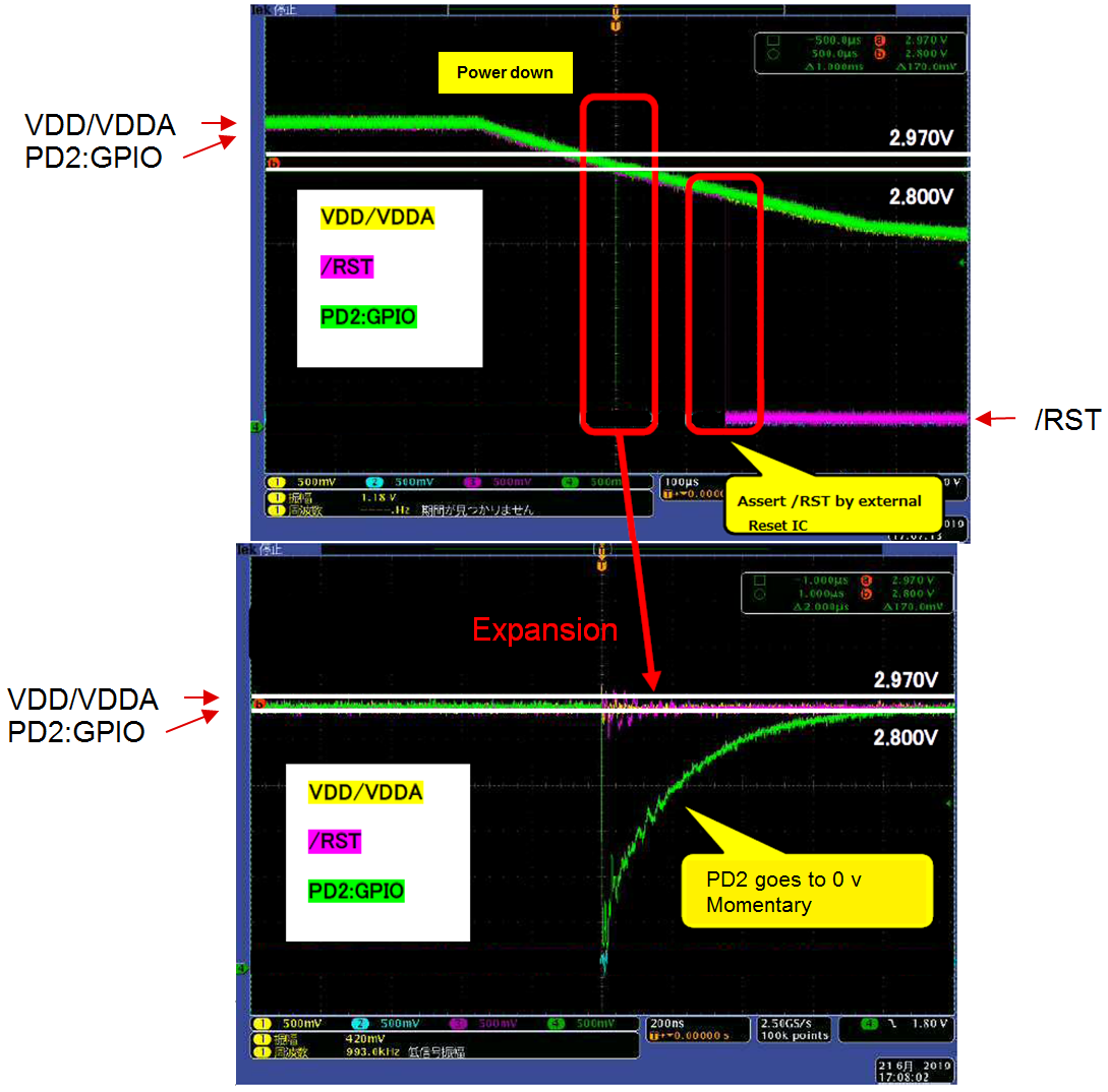
Although Our customer was evaluating their system with TM4C1290NCZAD , our customer noticed PD2 terminal indicated low(0V) for split second during system power down. Also, This behavior was observed when /RST was just asserted. I believe BOR(Brown-Out Reset) seems to occur since VDD show around 2.8V. as the result, PD2 is configured as default setting. Can we have your Expert’s comments on this behavior?

Also, if possible, could you elaborate how to avoid this unexpected low transaction , please?

Best regards,

Miyazaki

  • Hello Miyazaki-san,

    Had to dig for a bit to find the information behind it, but from what I discovered it looks like the 'glitch' has to do with the order of TivaWare configurations. So it's not actually directly due to the Reset itself, but what happens after the reset with how the pin is reconfigured, at least from what I can see.

    The post that explained the solution is here: https://e2e.ti.com/support/microcontrollers/other/f/908/p/506945/1839761#1839761

    On my end, I tested using a pull-up on a GPIO I set to Open Drain and observed it being pulled low on reset. Then I implemented the configuration used in that post, and I no longer saw it getting pulled low. Based on this, I believe that the outlined combination of API's would solve the customers issue as well.

  • Hello Ralph,

    Thanks for sharing your solution. Also, I really appreciate your help since you tested it on your site. I will share your comments with our customer,soon. I’d like to wait for customer’s feedback. When I’ll be able to receive it , I’ll close this thread.

    Best regards,

    Miyazaki

  • Hello,


    Thank you for sharing information.


    We referred to above your comment, and changed configuration order.

    However, we have not seen any changing so far.


    Originally, we set register in the following turn.

    GPIOPadConfigSet(GPIO_PORTD_BASE, GPIO_PIN_2, GPIO_STRENGTH_8MA, GPIO_PIN_TYPE_OD);

    GPIODirModeSet(GPIO_PORTD_BASE, GPIO_PIN_2, GPIO_DIR_MODE_OUT);

    GPIOPinWrite(GPIO_PORTD_BASE, GPIO_PIN_2, GPIO_PIN_2) ;


    After referred your comment, we changed the turn.

    GPIODirModeSet(GPIO_PORTD_BASE, GPIO_PIN_2, GPIO_DIR_MODE_OUT);

    GPIOPinWrite(GPIO_PORTD_BASE, GPIO_PIN_2, GPIO_PIN_2) ;

    GPIOPadConfigSet(GPIO_PORTD_BASE, GPIO_PIN_2, GPIO_STRENGTH_8MA, GPIO_PIN_TYPE_OD);


    We also changed register RESBEHAVCTL.

    But there is still the small low pulse.


    Do you have any idea how to take off this small low pulse?

    I would appreciate it if you could give us some information.


    Best regards

  • While FAR from the vendor team - perhaps my firm's use of ARM MCUs from MULTIPLE VENDORS - casts a 'Broader & Even Deeper Net' and just may lead to the successful resolution of this issue.

    My team sees 3 quick approaches - ideally operating in concert (together) which are likely to resolve:

    • Using the 'updated' code (i.e. beginning w/ "GPIODirModeSet()")  EMPLOY SUFFICIENT DELAYS - PRIOR TO (EACH) of the Two Following FUNCTION CALLS!     As the "GPIODirModeSet()" call is relatively MAJOR - does it prove wise - to  'SO IMMEDIATELY follow it  w/other calls - minus ANY Delay?    Borderline obvious - yet warrants test & verification - does it not?   To the delay's value - start long (say (even) 100mS) - reduce (only) upon 'Noted Success'  - and then insure that the reduced delays remain wide enough so that the MCU's: Temperature, Process Variation, and Aging - ALL are accommodated!   
    • Employ a pull-up R of 10K - (200K is far too high)
    • Code past shown employed "GPIO_STRENGTH_2MA" - is it  'wise'  to alter (especially increase) that?    May I note - that  (past) working for another  'giant' Semi Firm - provisioning such multiple (especially higher) output current selections - rendered that circuit  MORE VULNERABLE to such 'glitches!'    Should '8mA' (the NEW Value imposed) be required -  ADD that value (only)  after the 'immediate issue at hand' is resolved.   (it proves always unwise to  'Add a new 'variable' - no matter how 'simple' - while such issues are being battled!')

    The 'effectivenness' of the MCU's Reset - prior to this code's running - also  merits investigation.   My group prefers (longer) rather than (shorter) 'time-periods' - while the MCU is w/in 'Reset.'   And proper 'MCU Reset ICs' - are known to behave more predictably - such should be evaluated - should they not?

    And to be most complete - what (other) code - if any - runs prior to these '3 updated function calls?'     Can those calls - by themselves - succeed w/out prior MCU Set-Up & Configuration?   (It is expected that - at minimum - the chosen 'Output Port' - must (first) be enabled.    (maybe)     And that code (if required) appears nowhere - in the past posting - nor here, now...

    The fact that  Vendor's Ralph - reports 'Success' - brings hope.   Perhaps his listing of his complete 'Code Test Sequence' (to include MCU Set-Up/Config) - would  bring 'ALL HERE' to an equal 'Playing Field' - that's much to be desired - is it not?   In addition - Ralph's description of his MCU's Reset Circuit - insures that (unfortunate & unsuspected) 'variations' are detected - and minimized.

    It is hoped that these suggestions are viewed as 'helpful' - and that they are 'given the chance' to Succeed...   (Can an outside idea - ever prove instructive and/or worthwhile?   Does 'NIH' still RULE?)   Our quick testing reveals 'No such 'Glitch Low' just post Reset - upon the first two of (3 other) brand ARM Cortex MCUs (one an M4 - the 2nd an M7.)   That 'speaks to something' - does it not?

  • Hello,

    I am at another TI site and won't get a chance to test again with an oscilloscope until tomorrow. Please await further details until then and sorry for the delay.

    And thanks cb1 for your added tests, I agree that posting full code after re-testing this case would prove valuable for all. On the topic of delays, I hadn't seen that they were needed in my case, but I'll play around with that a bit as well so see if there is any observations of worth.

  • Greetings Ralph,

    Now - may the crack-staff  'here' (cb1's - back-room HQ)  'Radio Mayday!'    "Houston - We've got a  (thus far)  'undetected'  problem!"

    The opening post here noted:    (staff suspects that  'this perhaps has been - lost in process!')

    "our customer noticed PD2 terminal indicated low(0V) for split second  during system power down.    Also, This behavior was observed when /RST was just asserted.

    Now that  (past thread)  - from which the (hoped for)  corrective code was  'pried/imported'  - to my group's mind - is 'unlikely' to resolve such, "Low Driving Glitch during 'System Power Down' - don't you agree?    

    It is suspected that the (past) 'code fix' - would have the best chance of succeeding  (only) after the 'Initial MCU Power on Reset!'    Thus - only ONE of this clients TWO demands - has been recognized - and has thus received - 'Resolution Efforts.'  

    Upon staff's/my 're-read' of the code w/in "GPIODirModeSet()" - we (now) believe our earlier belief: ('its 'being Major')  - was mistaken.    (As only 2 Registers are impacted - via first a logical OR followed by an AND - which should execute quickly/easily.)

    I'd ask that the poster (client) identify the 'Significance of the Power Down 'GPIO Drive to Zero' Glitch.   Is the 'Quad SPI Flash'  (the recipient of said glitch)  'really/notably' impacted?     (by its 'CS' - so briefly - driving low?   Has ANY  'SPI' data corruption occurred?)

    Sometimes one 'Casts one's  fishing-pole in the 'Wrong Stream.'    Might the (offending) glitch be absorbed  by a  'simple, external R-C network'  - especially as the 'Low-Driving Glitch' appears as a very short impulse and our User has (already) imposed 1/2 of  such  R-C network!   (via his 'damping' resistor - only a small, low ESR, ceramic cap is to be added!)   Also - so long as in compliance w/the MCU's GPIO spec - that  Quad SPI's 'Pull-Up' may be reduced in value - (even)  further 'compressing'  the  offending glitch's pulse width.

    [edit] 02:44 CST - - Adding these  3  items for client & vendor consideration:

    • Urge that 'ALL other'  Set-up and/or Configurations - forced upon PD2 - be first identified - then listed - then reviewed - with the goal being to prevent  (at least reduce) PD2 from being able to, 'Fast Attack!'    One such area would be Port_D's 'Slew Rate Control' Register(s).   (slew rate must be minimized!)    In addition - at least temporarily - reprogram Port_D from the AHB Bus to the (slower) APB Bus!   Any/all other registers - which tend to 'Lessen Port_D's speeded response - should be 'Set to the most slowed response possible.'
    • Might there be (something) 'Special' about PD2 - which renders it especially 'susceptible' - to such glitching?   (I'd carefully examine any/all 'special function and/or signal capability' - potentially assigned to PD2.)    Again - anything which potentially enables 'fast response or activation' - should be blocked.
    • Suggest as well - should those 2 items above 'fail' - that (other) of Port_D's GPIO be test/verified - to further detect the potential for a 'PD2' anomaly!    Should all pins w/in Port_D behave similarly - I'd move to another Port - and test that.

    More and clearer facts are required -  the ADDED analysis here   'Informs, Advises & Exposes'  an expanded set of Diagnostics - which past have proved 'highly successful...'

  • Yet another 'Method of Attack' to User's Issue dawns!    Not wishing to 'further burden' my post above - the latest suggestion is presented here.

    Tech Background: (boring - but likely worthwhile)

    In our BLDC Motor 'Controller Development'  - each of the Motor's Three Phases - is driven by a, 'Power FET pair.'    One FET Sourcing - the other Sinking - yet NEVER/EVER w/ANY Overlap!   (Vital as such overlap would, 'Route the current between both FETs (path of least resistance!)     Most always leading to their INSTANT DESTRUCTION - and sometimes - even FIRE!    This happens (or past happened) so regularly that this destructive current flow is noted as, 'SHOOT-THRU!'   (and major efforts are deployed to 'avoid it.')

    The usual '20KHz & up' switching speeds - and FET currents  (sometimes) > 80A RMS - make the 'Prevention of Shoot-Thru' - Priority ONE!   The 'normal/customary' preventive measures include:

    • implementation of 'dead-band'  (method in which a programmable 'delay' is 'auto-inserted' - prior to the TURN-ON - of (either) Power FET.   (i.e. both the High & Low Side FETs)   The dead-band's delay seeks to (reasonably) insure that the  'FET Ordered OFF' - has (really) Turned OFF (i.e. had sufficient time to turn off) - prior to its complementary FET - Turning ON!
    • beyond 'dead-band' (a feature 'built-in' to this vendor's MCUs - BTW) there are 'Circuit Implementations' which (further) ENHANCE - Power FET's Turn OFF.   It is 'one of these techniques' - which I believe - may resolve our poster's (Glitch) issue.

    FET Turn Off may be enhanced (i.e. speeded) by, 'Providing a 'higher current-flow path' to the Power FET's Gate  - during the Turn Off interval!   (i.e. the 'charge' upon the FET's gate is more effectively removed via such  INCREASED 'gate current'  flow.)    This provides a  (likely) 'clue' - to the resolution of poster's unwanted (drive to low) glitch.

    Proposed then is a 'Dual Path' circuit implementation - which, 'Enables High-Speed assertion of 'Logic High' upon the SPI's Chip Select'  - yet (effectively) 'Enables (only) far Lower-Speed assertion of 'Logic Low!'   In theory - this 'external' circuitry serves as a 'corrective, Glitch Eater.'

    However - thinking (even) further/deeper - the 'Logic High' path (already exists - via the pull-up R)  - which I earlier suggested be, 'lowered in value.'   And that 'lowered R value holds.'   It remains (only) then - to prevent the (still) Glitching PD2 (if in fact - that glitch persists) from being 'felt' - at the SPI's Chip-Select.   That can be accomplished by:

    • (*) inserting a 'steering diode' (ideally Schottky - cathode toward PD2) in series with an increased value 'damping resistor.'
    • and adding the earlier suggested 'low ESR  ceramic capacitor' right at the SPI device's Chip Select pin.   (some experimentation required - suspect 0.01µF (may) prove a good start)

    This circuit intends to (still) enable - MCU pin 'PD2'  - to 'Command/Control' the SPI Chip Select.   Yet it reduces any 'Low Driving' glitch effect - which is 'unwanted' and generated by PD2.    it should be noted that the 'Combination of  the, 'SPI's Pull-Up Resistor and the user's 'Damping' resistor form a Voltage Divider - and those relative resistor values must thus be chosen such that:

    • the Glitch emanating from PD2 (should it still remain) is substantially 'weakened' - ideally 'not seen/felt' - by the SPI's Chip Select
    • the (proper) command of PD2 to a legitimate Logic Low - is indeed maintained at the SPI's Chip Select.    Some experimentation may be required to chose a 'proper pairing' of the 'Pull-Up R AND damping resistor's values.

    Crack staff's arrival (07:30 CST) may enable schematic - should this 'manifesto' - require (even) further detail.

    (*)   It IS 03:xx - that 'steering diode' is not needed - as PD2 - when in 'Open Drain' mode - can only 'Pull Down.'    When 'more normally'  - employing a GPIO as 'Push-Pull' Output (enabling both Sourcing & Sinking)  - then the 'steering diode' proves appropriate.   (and necessary - again Not the case - here...)

    This reporter is (now) 'Out of Ideas' ... and exits ... best of luck to our poster.   (who it is hoped - has mastered the art of Verifying (only) that post which (truly) resolved the issue - not his/her own - which (merely) confirmed the 'resolution efforts' of another.)

  • Hello,

    So after further testing, it looks like this workaround only solves the issue for situations with the GPIO drive strength being low. Only GPIO_STRENGTH_2MA works for this workaround.

    For other drive strength levels, the pin is seen going low on Reset.

    I have not found another workaround to circumvent this behavior yet.

    Regarding your use case, to echo a couple of cb1's questions:

    1. Why do you need the higher drive strength? I feel that a chip select shouldn't need that higher level of drive current.
    2. Is there a negative impact observed with the CS pin being toggled?

    To cb1, I actually had tested this based on device Reset. It's a very odd quirk where on reset, there is a very short moment where the pin is forced low before the pull-up restores it high. It's very brief, and only occurs on Reset. Before configuration and during configuration, the pin will remain high. This behavior isn't isolated to one pin, and I was able to replicate it on other pins that have pull-ups on them.

    One thing I haven't tried yet is seeing if there is a relationship between the resistance of the pull-up resistor, the drive strength of the GPIO, and the glitch.

  • Hello Ralph,

    Appears that you've had a safe trip back to 'home-base.'    Team/I fly tomorrow - yet another - 'Working Weekend!'    (but w/water - and sailboats - and submersibles - thus 'almost fun.'

    Now may the record show that one here (that would be moi) back on 23 July 12:04 - was the first to propose that the drive strength be limited to 2mA - NOT the 8mA - which this user deployed.

    cb1_mobile said:
    Code past shown employed "GPIO_STRENGTH_2MA" - is it  'wise'  to alter (especially increase) that?    May I note - that  (past) working for another  'giant' Semi Firm - provisioning such multiple (especially higher) output current selections - rendered that circuit  MORE VULNERABLE to such 'glitches!'

    You asked additionally, "if there was negative impact resulting from the SPI CS being toggled" - which I had earlier asked - to 'Silence.'   Appears that 'not always' do the outsiders 'Miss their Mark' - even though (so often) treated that way by user's who 'prefer only vendor agents...'

    BTW - the Glitch Filter I detailed should (completely) suppress this signal - at the cost of ONE small ceramic Cap - - (sometimes) simple Hardware RULES!

  • Hello Ralph,

    Thanks for your advice.

    Our customer was able to confirm that this glitch signal does not issue negative impact for SPI Flash which customer used. therefore, I'd like to close this ticket. I mean, customer also received Memory vender's comments. 

    Best regards,

    Miyazaki

  • Hello Ralph,

    The 'travesty' of 'Misunderstood & Misplaced Verify' continues in full-force - and is on full display - right here.

    NO 'LIKE' - NO (proper/deserved) 'VERIFY' - can there exist a better means to, 'REMOVE OUTSIDER PARTICIPATION?'

    Kindly note that my team is (highly) composed of,  'IMPRESSIONABLE, YOUNG COLLEGE STUDENTS/NEW GRADS!'    (So Highly Skilled/Motivated - as their efforts here revealed) - and they are (both) properly frustrated & disappointed - as their 'excellent analysis & recommendations'  have been, 'entirely Passed Over!'    That cannot be right - and conveys a TERRIBLE Impression of your firm - does it not?

    Should it not be made far more clearly/effectively  - that (ONLY) that post - which properly detected & then led to the 'ISSUE'S RESOLUTION' - is the again (only) one which should receive the, 'This Post RESOLVED my ISSUE AWARD!     Poster's (continue) to 'Verify their own posting' - which inevitably is incorrect - as their own post 'Simply Confirms the (Insightful & Resolving) work of the 'Unrecognized Other!'

    Might this (long) lingering issue be reduced (ideally eliminated)  - by the use of  'Amplifying - even (pardon) Directing Language' which 'Emphasizes that ONLY that Posting which ENABLED the ISSUE'S RESOLUTION' - is to be marked as, Verifying!    (RESOLVING - proves  superior to 'Verify'  - does it not?)

    The simple advisory - "Do not mark your own post as 'Verifying' - unless your post has (actually) identified & resolved the listed issue!" - seems a simple yet (vastly improved) guide - does it not?